Home > Press > Major leap towards graphene for solar cells - Surprising result: Graphene retains its properties even when coated with silicon
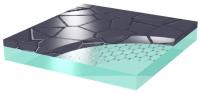 |
| Graphene was deposited onto a glass substrate. The ultrathin layer is but one atomic layer thick (0.3 Angstr�m, or 0.03 nanometers), although charge carriers are able to move about freely within this layer. This property is retained even if the graphene layer is covered with amorphous or polycrystalline silicon.
Credit: Marc A. Gluba/HZB |
Abstract:
Graphene has extreme conductivity and is completely transparent while being inexpensive and nontoxic. This makes it a perfect candidate material for transparent contact layers for use in solar cells to conduct electricity without reducing the amount of incoming light - at least in theory. Whether or not this holds true in a real world setting is questionable as there is no such thing as "ideal" graphene - a free floating, flat honeycomb structure consisting of a single layer of carbon atoms: interactions with adjacent layers can change graphene's properties dramatically.
Major leap towards graphene for solar cells - Surprising result: Graphene retains its properties even when coated with silicon
Berlin, Germany | Posted on October 8th, 2013"We examined how graphene's conductive properties change if it is incorporated into a stack of layers similar to a silicon based thin film solar cell and were surprised to find that these properties actually change very little," Marc Gluba explains. To this end, they grew graphene on a thin copper sheet, next transferred it to a glass substrate, and finally coated it with a thin film of silicon. They examined two different versions that are commonly used in conventional silicon thin-film technologies: one sample contained an amorphous silicon layer, in which the silicon atoms are in a disordered state similar to a hardened molten glas; the other sample contained poly-crystalline silicon to help them observe the effects of a standard crystallization process on graphene's properties.
Even though the morphology of the top layer changed completely as a result of being heated to a temperature of several hundred degrees C, the graphene is still detectable. "That's something we didn't expect to find, but our results demonstrate that graphene remains graphene even if it is coated with silicon," says Norbert Nickel.
Their measurements of carrier mobility using the Hall-effect showed that the mobility of charge carriers within the embedded graphene layer is roughly 30 times greater than that of conventional zinc oxide based contact layers. Says Gluba: "Admittedly, it's been a real challenge connecting this thin contact layer, which is but one atomic layer thick, to external contacts. We're still having to work on that." Adds Nickel: "Our thin film technology colleagues are already pricking up their ears and wanting to incorporate it." The researchers obtained their measurements on one square centimeter samples, although in practice it is feasible to coat much larger areas than that with graphene.
###
This work was recently published in Applied Physics Letters Vol. 103, 073102 (2013).
Authors: M. A. Gluba, D. Amkreutz, G. V. Troppenz, J. Rappich, and N. H. Nickel
doi: 10.1063/1.4818461
####
For more information, please click here
Contacts:
Antonia R�tger
49-308-062-43733
Copyright © Helmholtz-Zentrum Berlin f�r Materialien und Energie
If you have a comment, please Contact us.Issuers of news releases, not 7th Wave, Inc. or Nanotechnology Now, are solely responsible for the accuracy of the content.
Bookmark:


| Related News Press |
News and information
![]() Quantum computer improves AI predictions April 17th, 2026
Quantum computer improves AI predictions April 17th, 2026
![]() Flexible sensor gains sensitivity under pressure April 17th, 2026
Flexible sensor gains sensitivity under pressure April 17th, 2026
![]() A reusable chip for particulate matter sensing April 17th, 2026
A reusable chip for particulate matter sensing April 17th, 2026
![]() Detecting vibrational quantum beating in the predissociation dynamics of SF6 using time-resolved photoelectron spectroscopy April 17th, 2026
Detecting vibrational quantum beating in the predissociation dynamics of SF6 using time-resolved photoelectron spectroscopy April 17th, 2026
Thin films
![]() Tiny nanosheets, big leap: A new sensor detects ethanol at ultra-low levels January 30th, 2026
Tiny nanosheets, big leap: A new sensor detects ethanol at ultra-low levels January 30th, 2026
Graphene/ Graphite
![]() Electrifying results shed light on graphene foam as a potential material for lab grown cartilage June 6th, 2025
Electrifying results shed light on graphene foam as a potential material for lab grown cartilage June 6th, 2025
![]() Breakthrough in proton barrier films using pore-free graphene oxide: Kumamoto University researchers achieve new milestone in advanced coating technologies September 13th, 2024
Breakthrough in proton barrier films using pore-free graphene oxide: Kumamoto University researchers achieve new milestone in advanced coating technologies September 13th, 2024
Discoveries
![]() Quantum computer improves AI predictions April 17th, 2026
Quantum computer improves AI predictions April 17th, 2026
![]() Flexible sensor gains sensitivity under pressure April 17th, 2026
Flexible sensor gains sensitivity under pressure April 17th, 2026
![]() A reusable chip for particulate matter sensing April 17th, 2026
A reusable chip for particulate matter sensing April 17th, 2026
![]() Detecting vibrational quantum beating in the predissociation dynamics of SF6 using time-resolved photoelectron spectroscopy April 17th, 2026
Detecting vibrational quantum beating in the predissociation dynamics of SF6 using time-resolved photoelectron spectroscopy April 17th, 2026
Announcements
![]() A fundamentally new therapeutic approach to cystic fibrosis: Nanobody repairs cellular defect April 17th, 2026
A fundamentally new therapeutic approach to cystic fibrosis: Nanobody repairs cellular defect April 17th, 2026
![]() UC Irvine physicists discover method to reverse �quantum scrambling� : The work addresses the problem of information loss in quantum computing system April 17th, 2026
UC Irvine physicists discover method to reverse �quantum scrambling� : The work addresses the problem of information loss in quantum computing system April 17th, 2026
Interviews/Book Reviews/Essays/Reports/Podcasts/Journals/White papers/Posters
![]() A fundamentally new therapeutic approach to cystic fibrosis: Nanobody repairs cellular defect April 17th, 2026
A fundamentally new therapeutic approach to cystic fibrosis: Nanobody repairs cellular defect April 17th, 2026
![]() UC Irvine physicists discover method to reverse �quantum scrambling� : The work addresses the problem of information loss in quantum computing system April 17th, 2026
UC Irvine physicists discover method to reverse �quantum scrambling� : The work addresses the problem of information loss in quantum computing system April 17th, 2026
Energy
![]() Sensors innovations for smart lithium-based batteries: advancements, opportunities, and potential challenges August 8th, 2025
Sensors innovations for smart lithium-based batteries: advancements, opportunities, and potential challenges August 8th, 2025
![]() Simple algorithm paired with standard imaging tool could predict failure in lithium metal batteries August 8th, 2025
Simple algorithm paired with standard imaging tool could predict failure in lithium metal batteries August 8th, 2025
Solar/Photovoltaic
![]() Spinel-type sulfide semiconductors to operate the next-generation LEDs and solar cells For solar-cell absorbers and green-LED source October 3rd, 2025
Spinel-type sulfide semiconductors to operate the next-generation LEDs and solar cells For solar-cell absorbers and green-LED source October 3rd, 2025
![]() KAIST researchers introduce new and improved, next-generation perovskite solar cell November 8th, 2024
KAIST researchers introduce new and improved, next-generation perovskite solar cell November 8th, 2024
![]() Groundbreaking precision in single-molecule optoelectronics August 16th, 2024
Groundbreaking precision in single-molecule optoelectronics August 16th, 2024
![]() Development of zinc oxide nanopagoda array photoelectrode: photoelectrochemical water-splitting hydrogen production January 12th, 2024
Development of zinc oxide nanopagoda array photoelectrode: photoelectrochemical water-splitting hydrogen production January 12th, 2024
|
|
||
|
|
||
| The latest news from around the world, FREE | ||
|
|
||
|
|
||
| Premium Products | ||
|
|
||
|
Only the news you want to read!
Learn More |
||
|
|
||
|
Full-service, expert consulting
Learn More |
||
|
|
||