Home > Press > Bruker Introduces New LumiMap Electroluminescence Tool for Optical and Electrical Characterization on Epi Wafers for HB-LEDs: New Technology Delivers Fast and Repeatable Measurements for Epi Process Quality Control
 |
Abstract:
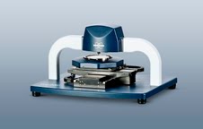
Today at the 15th China International Optoelectronic Exposition (CIOE 2013), Bruker introduced the new LumiMap™ Electroluminescence System for uncompromised HB-LED epi wafer process metrology. LumiMap joins a suite of other successful Bruker HB-LED epi metrology tools, and it incorporates many of the advanced features of Bruker's flagship metrology products. Proprietary, patent-pending features of the new system include the durable conducting probe, a unique wafer edge contact solution, and advanced I-V curve modeling for accurate and repeatable forward voltage value measurement. These features enable LumiMap to deliver the most accurate and repeatable forward and reverse IV characteristics, spectral intensity, wavelength and spectral width measurements on 2- to 6-inch epi wafers, with a wide range of current settings.
Bruker Introduces New LumiMap Electroluminescence Tool for Optical and Electrical Characterization on Epi Wafers for HB-LEDs: New Technology Delivers Fast and Repeatable Measurements for Epi Process Quality Control
Shenzhen, China | Posted on September 5th, 2013"LumiMap provides more accurate and reliable electrical and optical epi wafer measurements than the traditional indium dot method," said Dr. Ryan Lee, Executive VP and CTO of Foshan Nationstar Optoelectronics Co. Ltd. "A reliable electro-luminescence quality check immediately after MOCVD will help us further improve epi wafer yield and reduce costs."
"Bruker is pleased to bring a new technology solution to HB-LED manufacturing, rounding out our other HB-LED metrology technologies in 3D optical microscopy, atomic force microscopy and XRD/XRF for PSS wafers and epi wafer multi-quantum layer characterization," said Dr. Xiaomei Li, Vice President of Segment Marketing of the Bruker Nano Surfaces division. "LumiMap ideally serves stringent HB-LED manufacturing cost reduction goals at a time when the industry is poised for unprecedented growth."
"LumiMap electroluminescence technology fills the current lack of fast, non-destructive, reliable and repeatable optical and electrical measurement solutions to improve epi wafer yield and LED device quality at the epi wafer stage," added Robert M. Loiterman, Executive Vice President and General Manager of Bruker's Stylus and Optical Metrology Business. "With LumiMap, the HB-LED industry can now get accurate electrical and optical feedback in minutes rather than days, reducing scrap events and operating costs."
####
About Bruker Corporation
Bruker is a leading provider of high-performance scientific instruments and solutions for molecular and materials research, as well as for diagnostics, industrial and applied analysis.
About LumiMap
LumiMap is a value-oriented alternative to conventional, multistep, operator-dependent indium dot methods of epi (made by epitaxial growth) wafer characterization. The system features rapid, non-destructive, no post measurement chemical cleaning, software-controlled measurement locations, and repeatable optical and electrical measurement capabilities through forming a temporary LED (light-emitting diode) device on an epi wafer. The results obtained by LumiMap are well correlated with those on the final HB-LED (high brightness LED) device, providing an early warning of process shifts, which in turn reduces the risk of expensive scrap events and improves yields. Simple wafer exchange and intuitive software provides the industry’s easiest to use interface for production quality control, as well as epi process development. The long measurement lifetime of the proprietary conducting probe meets the strictest industry cost of ownership requirements.
For more information, please click here
Contacts:
Stephen Hopkins
Marketing Communications
Bruker Nano Surfaces
T: +1 (520) 741-1044 x1022
Copyright © Bruker Corporation
If you have a comment, please Contact us.Issuers of news releases, not 7th Wave, Inc. or Nanotechnology Now, are solely responsible for the accuracy of the content.
Bookmark:


| Related News Press |
News and information
![]() Quantum computer improves AI predictions April 17th, 2026
Quantum computer improves AI predictions April 17th, 2026
![]() Flexible sensor gains sensitivity under pressure April 17th, 2026
Flexible sensor gains sensitivity under pressure April 17th, 2026
![]() A reusable chip for particulate matter sensing April 17th, 2026
A reusable chip for particulate matter sensing April 17th, 2026
![]() Detecting vibrational quantum beating in the predissociation dynamics of SF6 using time-resolved photoelectron spectroscopy April 17th, 2026
Detecting vibrational quantum beating in the predissociation dynamics of SF6 using time-resolved photoelectron spectroscopy April 17th, 2026
Display technology/LEDs/SS Lighting/OLEDs
![]() Spinel-type sulfide semiconductors to operate the next-generation LEDs and solar cells For solar-cell absorbers and green-LED source October 3rd, 2025
Spinel-type sulfide semiconductors to operate the next-generation LEDs and solar cells For solar-cell absorbers and green-LED source October 3rd, 2025
![]() Efficient and stable hybrid perovskite-organic light-emitting diodes with external quantum efficiency exceeding 40 per cent July 5th, 2024
Efficient and stable hybrid perovskite-organic light-emitting diodes with external quantum efficiency exceeding 40 per cent July 5th, 2024
Chip Technology
![]() A reusable chip for particulate matter sensing April 17th, 2026
A reusable chip for particulate matter sensing April 17th, 2026
![]() Metasurfaces smooth light to boost magnetic sensing precision January 30th, 2026
Metasurfaces smooth light to boost magnetic sensing precision January 30th, 2026
Announcements
![]() A fundamentally new therapeutic approach to cystic fibrosis: Nanobody repairs cellular defect April 17th, 2026
A fundamentally new therapeutic approach to cystic fibrosis: Nanobody repairs cellular defect April 17th, 2026
![]() UC Irvine physicists discover method to reverse ‘quantum scrambling’ : The work addresses the problem of information loss in quantum computing system April 17th, 2026
UC Irvine physicists discover method to reverse ‘quantum scrambling’ : The work addresses the problem of information loss in quantum computing system April 17th, 2026
Tools
![]() Metasurfaces smooth light to boost magnetic sensing precision January 30th, 2026
Metasurfaces smooth light to boost magnetic sensing precision January 30th, 2026
![]() From sensors to smart systems: the rise of AI-driven photonic noses January 30th, 2026
From sensors to smart systems: the rise of AI-driven photonic noses January 30th, 2026
![]() Japan launches fully domestically produced quantum computer: Expo visitors to experience quantum computing firsthand August 8th, 2025
Japan launches fully domestically produced quantum computer: Expo visitors to experience quantum computing firsthand August 8th, 2025
Events/Classes
![]() Institute for Nanoscience hosts annual proposal planning meeting May 16th, 2025
Institute for Nanoscience hosts annual proposal planning meeting May 16th, 2025
![]() A New Blue: Mysterious origin of the ribbontail ray’s electric blue spots revealed July 5th, 2024
A New Blue: Mysterious origin of the ribbontail ray’s electric blue spots revealed July 5th, 2024
![]() Researchers demonstrate co-propagation of quantum and classical signals: Study shows that quantum encryption can be implemented in existing fiber networks January 20th, 2023
Researchers demonstrate co-propagation of quantum and classical signals: Study shows that quantum encryption can be implemented in existing fiber networks January 20th, 2023
|
|
||
|
|
||
| The latest news from around the world, FREE | ||
|
|
||
|
|
||
| Premium Products | ||
|
|
||
|
Only the news you want to read!
Learn More |
||
|
|
||
|
Full-service, expert consulting
Learn More |
||
|
|
||