Home > Press > Penn develops computer model that will help design flexible touchscreens
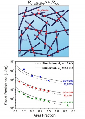 |
| Researchers simulate electrical resistances (lines) to match experimental data (points) and extract the contact resistance. |
Abstract:
Electronic devices with touchscreens are ubiquitous, and one key piece of technology makes them possible: transparent conductors. However, the cost and the physical limitations of the material these conductors are usually made of are hampering progress toward flexible touchscreen devices.
Penn develops computer model that will help design flexible touchscreens
Philadelphia, PA | Posted on September 5th, 2013Fortunately, a research collaboration between the University of Pennsylvania and Duke University has shown a new a way to design transparent conductors using metal nanowires that could enable less expensive � and flexible � touchscreens.
The research was conducted by graduate student Rose Mutiso, undergraduate Michelle Sherrott and professor Karen Winey, all of the Department of Materials Science and Engineering in Penn's School of Engineering and Applied Science. They collaborated with graduate student Aaron Rathmell, and professor Benjamin Wiley of Duke's Department of Chemistry.
Their study was published in the journal ACS Nano.
The current industry-standard material for making transparent conductors is indium tin oxide, or ITO, which is deposited as two thin layers on either side of a separator film. Contact, in the form of a fingertip or a stylus, changes the electrical resistance between the two ITO layers enough so that the device can register where the user is touching. While this material performs well, its drawbacks have led industrial and academic researchers to look for alternatives.
"There are two problems with ITO; indium is relatively rare, so its cost and availability are erratic, and, more importantly for flexible devices, it's brittle," Winey said. "We'd like to make touchscreens that use a network of thin, flexible nanowires, but predicting and optimizing the properties of these nanoscale networks has been a challenge."
Metal nanowires are increasingly inexpensive to make and deposit; they are suspended in a liquid and can easily be painted or sprayed onto a flexible or rigid substrate, rather than grown in vacuum as is the case for ITO. The challenge stems from the fact that this process forms a random network, rather than a uniform layer like ITO.
A uniform sheet's overall quality in this context depends on only two parameters, both of which can be reliably derived from the bulk material's properties: its transparency, which should be high, and its overall electrical resistance, which should be low. To determine the electrical properties for a network of nanowires, however, one needs to know the nanowires' length and diameter, the area they cover and a property known as contact resistance, which is the amount of resistance that results from electrons traveling from one wire to another. The details of how these four independent parameters impact the electrical and optical properties of nanowire networks have been unclear.
"What this means is that people will synthesize nanowires, deposit them in a network, measure the network's overall electrical resistance and optical properties and then claim victory when they get a good one," Winey said. "The problem is that they don't know why the good ones are good, and, worse, they don't necessarily know why the bad ones are bad."
For example, low overall resistance could be the result of a particular synthesis method that produced a few unexpectedly long nanowires, or a processing method that reduced the contact resistance between nanowires. Without a way of isolating these factors, researchers can't determine which combination of parameters will be most successful.
Winey's group has previously worked on simulating nanowire networks in three-dimensional nanocomposites, particularly the number of nanowires it takes to ensure there is a connected path from one end of the system to the other. Duke's Wiley took note of this work and contacted Winey, asking her if she would be interested in developing two-dimensional simulations that could be applied to data from silver nanowire networks his group had fabricated.
With Wiley's group able to provide the nanowire length, diameter and area fraction of their networks, Winey's team was able to use the simulation to work backward from the network's overall electrical resistance to uncover the elusive contact resistance. Alternative methods for finding the contact resistance are laborious and incompatible with typical network processing methods.
"Once we have reliable and relevant contact resistances, we can start asking how we can improve the overall sheet resistance by changing the other variables," Mutiso said. "In playing with this simulation, we can see how much better our networks get when we increase the length of the nanowires, for example."
The Penn team's simulation provides further evidence for each variable's role in the overall network's performance, helping the researchers home in on the right balance of traits for specific applications. Increasing the coverage area of nanowires, for example, always decreases the overall electrical resistance, but it also decreases optical transparency; as more and more nanowires are piled on the networks appear gray, rather than transparent.
"For specific applications and different types of nanowires, the optimal area fraction is going to be different," Winey said. "This simulation shows us how many nanowires we need to apply to reach the Goldilocks zone where you get the best mix of transparency and resistance."
Future collaborations between Winey's team at Penn and the Wiley group at Duke will use this simulation to test the effect of different processing techniques on nanowires, pinpointing the effect various post-deposition processing methods has on contact resistance and ultimately on overall sheet resistance.
"We can now make rational comparisons between different wires, as well as different processing methods for different wires, to find the lowest contact resistance independent of nanowire length, diameter and area fraction," Winey said. "Now that we know where all the levers are, we can start adjusting them one at a time."
In the next generation of modeling studies, the Penn team will consider several additional parameters that factor into the performance of nanowire networks for transparent conductors, including nanowire orientation, to mimic nanowire networks produced by various continuous deposition methods, as well as the degree to which individual nanowires vary in length or diameter.
The research was supported by the National Science Foundation and Penn's Materials Science Research and Engineering Center.
Michelle Sherrott is now a doctoral student in materials science at the California Institute of Technology.
####
For more information, please click here
Contacts:
Evan Lerner
215-573-6604
Copyright © University of Pennsylvania
If you have a comment, please Contact us.Issuers of news releases, not 7th Wave, Inc. or Nanotechnology Now, are solely responsible for the accuracy of the content.
Bookmark:


| Related Links |
| Related News Press |
News and information
![]() Quantum computer improves AI predictions April 17th, 2026
Quantum computer improves AI predictions April 17th, 2026
![]() Flexible sensor gains sensitivity under pressure April 17th, 2026
Flexible sensor gains sensitivity under pressure April 17th, 2026
![]() A reusable chip for particulate matter sensing April 17th, 2026
A reusable chip for particulate matter sensing April 17th, 2026
![]() Detecting vibrational quantum beating in the predissociation dynamics of SF6 using time-resolved photoelectron spectroscopy April 17th, 2026
Detecting vibrational quantum beating in the predissociation dynamics of SF6 using time-resolved photoelectron spectroscopy April 17th, 2026
Flexible Electronics
![]() Flexible sensor gains sensitivity under pressure April 17th, 2026
Flexible sensor gains sensitivity under pressure April 17th, 2026
![]() Flexible electronics integrated with paper-thin structure for use in space January 17th, 2025
Flexible electronics integrated with paper-thin structure for use in space January 17th, 2025
Display technology/LEDs/SS Lighting/OLEDs
![]() Spinel-type sulfide semiconductors to operate the next-generation LEDs and solar cells For solar-cell absorbers and green-LED source October 3rd, 2025
Spinel-type sulfide semiconductors to operate the next-generation LEDs and solar cells For solar-cell absorbers and green-LED source October 3rd, 2025
Govt.-Legislation/Regulation/Funding/Policy
![]() Quantum computer improves AI predictions April 17th, 2026
Quantum computer improves AI predictions April 17th, 2026
![]() Metasurfaces smooth light to boost magnetic sensing precision January 30th, 2026
Metasurfaces smooth light to boost magnetic sensing precision January 30th, 2026
![]() New imaging approach transforms study of bacterial biofilms August 8th, 2025
New imaging approach transforms study of bacterial biofilms August 8th, 2025
Discoveries
![]() Quantum computer improves AI predictions April 17th, 2026
Quantum computer improves AI predictions April 17th, 2026
![]() Flexible sensor gains sensitivity under pressure April 17th, 2026
Flexible sensor gains sensitivity under pressure April 17th, 2026
![]() A reusable chip for particulate matter sensing April 17th, 2026
A reusable chip for particulate matter sensing April 17th, 2026
![]() Detecting vibrational quantum beating in the predissociation dynamics of SF6 using time-resolved photoelectron spectroscopy April 17th, 2026
Detecting vibrational quantum beating in the predissociation dynamics of SF6 using time-resolved photoelectron spectroscopy April 17th, 2026
Announcements
![]() A fundamentally new therapeutic approach to cystic fibrosis: Nanobody repairs cellular defect April 17th, 2026
A fundamentally new therapeutic approach to cystic fibrosis: Nanobody repairs cellular defect April 17th, 2026
![]() UC Irvine physicists discover method to reverse �quantum scrambling� : The work addresses the problem of information loss in quantum computing system April 17th, 2026
UC Irvine physicists discover method to reverse �quantum scrambling� : The work addresses the problem of information loss in quantum computing system April 17th, 2026
|
|
||
|
|
||
| The latest news from around the world, FREE | ||
|
|
||
|
|
||
| Premium Products | ||
|
|
||
|
Only the news you want to read!
Learn More |
||
|
|
||
|
Full-service, expert consulting
Learn More |
||
|
|
||