Home > Press > Researchers discover breakthrough technique that could make electronics smaller and better
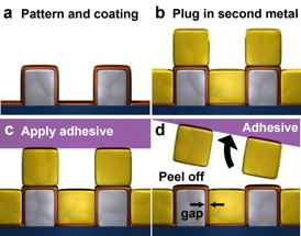 |
| In a breakthrough study to improve the manufacturing of optical and electronic devices, University of Minnesota researchers introduced a new patterning technology, atomic layer lithography, based on a layering technique at the atomic level. A layer of metal fills the nano-patterns over an entire wafer and simple Scotch Magic tape was used to remove the excess metal on the surface and expose the atomic scale nano-gaps. |
Abstract:
An international group of researchers from the University of Minnesota, Argonne National Laboratory and Seoul National University have discovered a groundbreaking technique in manufacturing nanostructures that has the potential to make electrical and optical devices smaller and better than ever before. A surprising low-tech tool of Scotch Magic tape ended up being one of the keys to the discovery.
Researchers discover breakthrough technique that could make electronics smaller and better
Minneapolis, MN | Posted on September 5th, 2013The research is published today in Nature Communications, an international online research journal.
Combining several standard nanofabrication techniques�with the final addition of the Scotch Magic tape�researchers at the University of Minnesota created extremely thin gaps through a layer of metal and patterned these tiny gaps over the entire surface of a four-inch silicon wafer. The smallest gaps were only one nanometer wide, much smaller than most researchers have been able to achieve. In addition, the widths of the gaps could be controlled on the atomic level. This work provides the basis for producing new and better nanostructures that are at the core of advanced electronic and optical devices.
One of the potential uses of nanometer-scale gaps in metal layers is to squeeze light into spaces much smaller than is otherwise possible. Collaborators at Seoul National University, led by Prof. Dai-Sik Kim, and Argonne National Laboratory, led by Dr. Matthew Pelton, showed that light could readily be squeezed through these gaps, even though the gaps are hundreds or even thousands of times smaller than the wavelength of the light used. Researchers are very interested in forcing light into small spaces because this is a way of boosting the intensity of the light. The collaborators found that the intensity inside the gaps is increased by as much as 600 million times.
"Our technology, called atomic layer lithography, has the potential to create ultra-small sensors with increased sensitivity and also enable new and exciting experiments at the nanoscale like we've never been able to do before," said Sang-Hyun Oh, one of the lead researchers on the study and a professor of electrical and computer engineering in the University of Minnesota's College of Science and Engineering. "This research also provides the basis for future studies to improve electronic and photonic devices."
One of the most surprising outcomes of the research is that Scotch Magic tape was one of the keys to the discovery. Etching one-nanometer-wide gaps into metals is not feasible with existing tools. Instead, the researchers in Oh's team constructed the nano-gaps by layering atomic-scale thin films on the sides of metal patterns and then capping the structure with another metal layer. No expensive patterning tools were needed to form the gaps this way, but it was challenging to remove the excess metals on top and expose the tiny gaps. During a frustrating struggle of trying to find a way to remove the metal films, University of Minnesota Ph.D. student and lead author of the study Xiaoshu Chen found that by using simple Scotch Magic tape, the excess metals could be easily removed.
"The Scotch tape works nicely, which was unexpected," said Oh. "Our technique is so simple yet can create uniform and ultra-small gaps like we've never been able to do before. We hope that it will rapidly be taken up by many researchers."
In addition to Oh and Chen, researchers involved in the study include a joint lead author Hyeong-Ryeol Park, who was a Ph.D. student at Seoul National University and is now a postdoc in Oh's group at the University of Minnesota; Matthew Pelton, a staff physicist at Argonne National Laboratory who is now a professor of physics at the University of Maryland, Baltimore County; Nathan Lindquist, a former Ph.D. student at the University of Minnesota who is now a professor of physics at Bethel University in St. Paul; Hyungsoon Im, a former electrical and computer engineering Ph.D. student who is now a postdoc at Harvard Medical School; and Xianji Piao, Yun Jung Kim, Jae Sung Ahn, Kwang Jun Ahn, Prof. Namkyoo Park, and Prof. Dai-Sik Kim, all from Seoul National University in Korea.
This research was funded by the U.S. Department of Defense (DARPA Young Faculty Award and the ONR Young Investigator Program), the U.S. Department of Energy and the National Research Foundation of Korea with capital equipment funding from the Minnesota Partnership for Biotechnology and Medical Genomics.
####
For more information, please click here
Contacts:
Rhonda Zurn
College of Science and Engineering
612-626-7959
Brooke Dillon
University News Service
(612) 624-2801
Copyright © University of Minnesota
If you have a comment, please Contact us.Issuers of news releases, not 7th Wave, Inc. or Nanotechnology Now, are solely responsible for the accuracy of the content.
Bookmark:


| Related Links |
| Related News Press |
News and information
![]() Quantum computer improves AI predictions April 17th, 2026
Quantum computer improves AI predictions April 17th, 2026
![]() Flexible sensor gains sensitivity under pressure April 17th, 2026
Flexible sensor gains sensitivity under pressure April 17th, 2026
![]() A reusable chip for particulate matter sensing April 17th, 2026
A reusable chip for particulate matter sensing April 17th, 2026
![]() Detecting vibrational quantum beating in the predissociation dynamics of SF6 using time-resolved photoelectron spectroscopy April 17th, 2026
Detecting vibrational quantum beating in the predissociation dynamics of SF6 using time-resolved photoelectron spectroscopy April 17th, 2026
Laboratories
![]() Researchers develop molecular qubits that communicate at telecom frequencies October 3rd, 2025
Researchers develop molecular qubits that communicate at telecom frequencies October 3rd, 2025
![]() A battery�s hopping ions remember where they�ve been: Seen in atomic detail, the seemingly smooth flow of ions through a battery�s electrolyte is surprisingly complicated February 16th, 2024
A battery�s hopping ions remember where they�ve been: Seen in atomic detail, the seemingly smooth flow of ions through a battery�s electrolyte is surprisingly complicated February 16th, 2024
Govt.-Legislation/Regulation/Funding/Policy
![]() Quantum computer improves AI predictions April 17th, 2026
Quantum computer improves AI predictions April 17th, 2026
![]() Metasurfaces smooth light to boost magnetic sensing precision January 30th, 2026
Metasurfaces smooth light to boost magnetic sensing precision January 30th, 2026
![]() New imaging approach transforms study of bacterial biofilms August 8th, 2025
New imaging approach transforms study of bacterial biofilms August 8th, 2025
Chip Technology
![]() A reusable chip for particulate matter sensing April 17th, 2026
A reusable chip for particulate matter sensing April 17th, 2026
![]() Metasurfaces smooth light to boost magnetic sensing precision January 30th, 2026
Metasurfaces smooth light to boost magnetic sensing precision January 30th, 2026
Discoveries
![]() Quantum computer improves AI predictions April 17th, 2026
Quantum computer improves AI predictions April 17th, 2026
![]() Flexible sensor gains sensitivity under pressure April 17th, 2026
Flexible sensor gains sensitivity under pressure April 17th, 2026
![]() A reusable chip for particulate matter sensing April 17th, 2026
A reusable chip for particulate matter sensing April 17th, 2026
![]() Detecting vibrational quantum beating in the predissociation dynamics of SF6 using time-resolved photoelectron spectroscopy April 17th, 2026
Detecting vibrational quantum beating in the predissociation dynamics of SF6 using time-resolved photoelectron spectroscopy April 17th, 2026
Announcements
![]() A fundamentally new therapeutic approach to cystic fibrosis: Nanobody repairs cellular defect April 17th, 2026
A fundamentally new therapeutic approach to cystic fibrosis: Nanobody repairs cellular defect April 17th, 2026
![]() UC Irvine physicists discover method to reverse �quantum scrambling� : The work addresses the problem of information loss in quantum computing system April 17th, 2026
UC Irvine physicists discover method to reverse �quantum scrambling� : The work addresses the problem of information loss in quantum computing system April 17th, 2026
Interviews/Book Reviews/Essays/Reports/Podcasts/Journals/White papers/Posters
![]() A fundamentally new therapeutic approach to cystic fibrosis: Nanobody repairs cellular defect April 17th, 2026
A fundamentally new therapeutic approach to cystic fibrosis: Nanobody repairs cellular defect April 17th, 2026
![]() UC Irvine physicists discover method to reverse �quantum scrambling� : The work addresses the problem of information loss in quantum computing system April 17th, 2026
UC Irvine physicists discover method to reverse �quantum scrambling� : The work addresses the problem of information loss in quantum computing system April 17th, 2026
Military
![]() Quantum engineers �squeeze� laser frequency combs to make more sensitive gas sensors January 17th, 2025
Quantum engineers �squeeze� laser frequency combs to make more sensitive gas sensors January 17th, 2025
![]() Chainmail-like material could be the future of armor: First 2D mechanically interlocked polymer exhibits exceptional flexibility and strength January 17th, 2025
Chainmail-like material could be the future of armor: First 2D mechanically interlocked polymer exhibits exceptional flexibility and strength January 17th, 2025
![]() Single atoms show their true color July 5th, 2024
Single atoms show their true color July 5th, 2024
![]() NRL charters Navy�s quantum inertial navigation path to reduce drift April 5th, 2024
NRL charters Navy�s quantum inertial navigation path to reduce drift April 5th, 2024
Research partnerships
![]() Lab to industry: InSe wafer-scale breakthrough for future electronics August 8th, 2025
Lab to industry: InSe wafer-scale breakthrough for future electronics August 8th, 2025
![]() HKU physicists uncover hidden order in the quantum world through deconfined quantum critical points April 25th, 2025
HKU physicists uncover hidden order in the quantum world through deconfined quantum critical points April 25th, 2025
|
|
||
|
|
||
| The latest news from around the world, FREE | ||
|
|
||
|
|
||
| Premium Products | ||
|
|
||
|
Only the news you want to read!
Learn More |
||
|
|
||
|
Full-service, expert consulting
Learn More |
||
|
|
||