Home > Press > Anasys' NIST users report on new AFM-IR nanoscale chemical imaging method used in the characterization of plasmonics
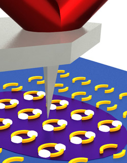 |
| Infrared laser light (purple) from below a sample (blue) excites ring shaped nanoscale plasmonic resonator structures (gold). Hot spots (white) form in the rings' gaps. In these hot spots, infrared absorption is enhanced, allowing for more sensitive chemical recognition. A scanning AFM tip detects the expansion of the underlying material in response to absorption of infrared light. Image reproduced courtesy of NIST |
Abstract:
Anasys Instruments announces a new application for AFM-IR to study as reported by research scientists in NIST publication "Tech Beat."
Anasys' NIST users report on new AFM-IR nanoscale chemical imaging method used in the characterization of plasmonics
Santa Barbara, CA | Posted on July 24th, 2013Researchers from the National Institute of Standards and Technology (NIST) and the University of Maryland have shown how to make nanoscale measurements of critical properties of plasmonic nanomaterials�the specially engineered nanostructures that modify the interaction of light and matter for a variety of applications, including sensors, cloaking (invisibility), photovoltaics and therapeutics. Their technique is one of the few that allows researchers to make actual physical measurements of these materials at the nanoscale without affecting the nanomaterial's function.
Plasmonic nanomaterials contain specially engineered conducting nanoscale structures that can enhance the interaction between light and an adjacent material, and the shape and size of such nanostructures can be adjusted to tune these interactions. Theoretical calculations are frequently used to understand and predict the optical properties of plasmonic nanomaterials, but few experimental techniques are available to study them in detail. Researchers need to be able to measure the optical properties of individual structures and how each interacts with surrounding materials directly in a way that doesn't affect how the structure functions.
"We want to maximize the sensitivity of these resonator arrays and study their properties," says lead researcher Dr Andrea Centrone. "In order to do that, we needed an experimental technique that we could use to verify theory and to understand the influence of nanofabrication defects that are typically found in real samples. Our technique has the advantage of being extremely sensitive spatially and chemically, and the results are straightforward to interpret."
The research team turned to photothermal induced resonance (PTIR), an emerging chemically specific materials analysis technique, and showed it can be used to image the response of plasmonic nanomaterials excited by infrared (IR) light with nanometer-scale resolution.
The team used PTIR, also known as AFM-IR*, to image the absorbed energy in ring-shaped plasmonic resonators. The nanoscale resonators focus the incoming IR light within the rings' gaps to create "hot spots" where the light absorption is enhanced, which makes for more sensitive chemical identification. For the first time, the researchers precisely quantified the absorption in the hot spots and showed that for the samples under investigation, it is approximately 30 times greater than areas away from the resonators.
The researchers also showed that plasmonic materials can be used to increase the sensitivity of IR and PTIR spectroscopy for chemical analysis by enhancing the local light intensity, and thereby, the spectroscopic signal. Their work further demonstrated the versatility of PTIR as a measurement tool that allows simultaneous measurement of a nanomaterial's shape, size, and chemical composition�the three characteristics that determine a nanomaterial's properties. Unlike many other methods for probing materials at the nanoscale, PTIR doesn't interfere with the material under investigation; it doesn't require the researcher to have prior knowledge about the material's optical properties or geometry; and it returns data that is more easily interpretable than other techniques that require separating the response of the sample from response of the probe.
*AFM-IR is a product from Anasys Instruments, Inc.
####
About Anasys Instruments
Anasys Instruments designs breakthrough, award-winning products that provide nanoscale probe based analytical techniques while providing high quality AFM imaging. We introduced the nano-TA in 2006 which launched the field of nanoscale thermal property measurement. In 2010, we introduced the nanoIR Platform which pioneered the field of nanoscale IR measurement. In 2012, Anasys introduced Lorentz Contact Resonance which developed the field of wideband nanoscale dynamic mechanical spectroscopy.
For more information, please click here
Contacts:
Anasys contact:
Roshan Shetty
Anasys Instruments Corporation
121 Gray Avenue, Suite 100
Santa Barbara
CA 93101 USA
Tel: +1 (805) 730-3310
Media contact:
Jezz Leckenby
Talking Science Limited
39 de Bohun Court
Saffron Walden
Essex CB10 2BA, UK
Tel +44 (0) 1799 521881
Mob +44 (0) 7843 012997
http://www.talking-science.com/
Copyright © Anasys Instruments
If you have a comment, please Contact us.Issuers of news releases, not 7th Wave, Inc. or Nanotechnology Now, are solely responsible for the accuracy of the content.
Bookmark:


| Related News Press |
News and information
![]() Quantum computer improves AI predictions April 17th, 2026
Quantum computer improves AI predictions April 17th, 2026
![]() Flexible sensor gains sensitivity under pressure April 17th, 2026
Flexible sensor gains sensitivity under pressure April 17th, 2026
![]() A reusable chip for particulate matter sensing April 17th, 2026
A reusable chip for particulate matter sensing April 17th, 2026
![]() Detecting vibrational quantum beating in the predissociation dynamics of SF6 using time-resolved photoelectron spectroscopy April 17th, 2026
Detecting vibrational quantum beating in the predissociation dynamics of SF6 using time-resolved photoelectron spectroscopy April 17th, 2026
Imaging
![]() Simple algorithm paired with standard imaging tool could predict failure in lithium metal batteries August 8th, 2025
Simple algorithm paired with standard imaging tool could predict failure in lithium metal batteries August 8th, 2025
![]() First real-time observation of two-dimensional melting process: Researchers at Mainz University unveil new insights into magnetic vortex structures August 8th, 2025
First real-time observation of two-dimensional melting process: Researchers at Mainz University unveil new insights into magnetic vortex structures August 8th, 2025
![]() New imaging approach transforms study of bacterial biofilms August 8th, 2025
New imaging approach transforms study of bacterial biofilms August 8th, 2025
Laboratories
![]() Researchers develop molecular qubits that communicate at telecom frequencies October 3rd, 2025
Researchers develop molecular qubits that communicate at telecom frequencies October 3rd, 2025
Govt.-Legislation/Regulation/Funding/Policy
![]() Quantum computer improves AI predictions April 17th, 2026
Quantum computer improves AI predictions April 17th, 2026
![]() Metasurfaces smooth light to boost magnetic sensing precision January 30th, 2026
Metasurfaces smooth light to boost magnetic sensing precision January 30th, 2026
![]() New imaging approach transforms study of bacterial biofilms August 8th, 2025
New imaging approach transforms study of bacterial biofilms August 8th, 2025
Announcements
![]() A fundamentally new therapeutic approach to cystic fibrosis: Nanobody repairs cellular defect April 17th, 2026
A fundamentally new therapeutic approach to cystic fibrosis: Nanobody repairs cellular defect April 17th, 2026
![]() UC Irvine physicists discover method to reverse �quantum scrambling� : The work addresses the problem of information loss in quantum computing system April 17th, 2026
UC Irvine physicists discover method to reverse �quantum scrambling� : The work addresses the problem of information loss in quantum computing system April 17th, 2026
Tools
![]() Metasurfaces smooth light to boost magnetic sensing precision January 30th, 2026
Metasurfaces smooth light to boost magnetic sensing precision January 30th, 2026
![]() From sensors to smart systems: the rise of AI-driven photonic noses January 30th, 2026
From sensors to smart systems: the rise of AI-driven photonic noses January 30th, 2026
![]() Japan launches fully domestically produced quantum computer: Expo visitors to experience quantum computing firsthand August 8th, 2025
Japan launches fully domestically produced quantum computer: Expo visitors to experience quantum computing firsthand August 8th, 2025
Research partnerships
![]() Lab to industry: InSe wafer-scale breakthrough for future electronics August 8th, 2025
Lab to industry: InSe wafer-scale breakthrough for future electronics August 8th, 2025
![]() HKU physicists uncover hidden order in the quantum world through deconfined quantum critical points April 25th, 2025
HKU physicists uncover hidden order in the quantum world through deconfined quantum critical points April 25th, 2025
|
|
||
|
|
||
| The latest news from around the world, FREE | ||
|
|
||
|
|
||
| Premium Products | ||
|
|
||
|
Only the news you want to read!
Learn More |
||
|
|
||
|
Full-service, expert consulting
Learn More |
||
|
|
||