Home > Press > Building 3D fractals on a nano scale
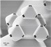 |
| Corners with nano pores |
Abstract:
It starts with one 3D structure with eight planes, an octahedron. This repeats itself to smaller octahedra: 625 after just four steps. At every corner of a new octahedron, a successive octahedron is formed. A truly fascinating 3D fractal ‘building' is formed on the micro and nano scale. It can be used for high performance filtering, for example. Scientists of the MESA+ Institute for Nanotechnology of the University of Twente in The Netherlands present these structures in the Journal of Micromechanics and Microengineering (JMM).
Building 3D fractals on a nano scale
Enschede, Netherlands | Posted on June 1st, 2013A fractal is a geometric structure that can repeat itself towards infinity. Zooming in on a fragment of it, the original structure becomes visible again. A major advantage of a 3D fractal is that the effective surface rises with every next step. Looking at the octahedra, after four steps the final structure is not much bigger than the original octahedron, but the effective surface has been multiplied by 6.5. The smallest octahedra are 300 nanometers in size, with on every corner a nano pore of 100 nanometer. Having 625 of these nano pores on a limited surface area, a very effective filer with low flow resistance is formed. The Dutch scientists also experiment with capturing living cells within these octahedral, to be able to study the interaction between the cells. Further interesting research is related to sending light through the octahedron structure: how will it interact?
Corner lithography
To be able to create the repeated 3D structure, the scientists developed a technique called ‘corner lithography''. At first, a pyramid form is etched in silicon. The next step is applying a layer of silicon nitride on the pyramid. After removing this subsequently, a tiny bit of nitride stays in the corner of the pyramid, functioning as a ‘stop'. When this is removed, the silicon underneath is etched through the tiny hole. Automatically, a structure is formed alongside the silicon crystal plane. This is the first octahedron, formed by ‘auto alignment'. The process is repeated with a new layer of silicon nitride. The size of the new octahedra is determined by the etch period. In this case, every octahedron in the next step is half the size of the previous one. The advantage of corner lithography is its relative simplicity. No advanced technology is needed to create each individual nano pore. On the contrary: in just four steps thousands of fractals, each having 625 tiny holes can be processed on a wafer, in parallel. More than four steps is also possible, but this places higher demands on the etching process.
The research has been performed in the Transducers Science and Technology group, which is part of the MESA+ Institute for Nanotechnology of the University of Twente.
####
For more information, please click here
Contacts:
Wiebe van der Veen
+31612185692
Copyright © AlphaGalileo
If you have a comment, please Contact us.Issuers of news releases, not 7th Wave, Inc. or Nanotechnology Now, are solely responsible for the accuracy of the content.
Bookmark:


| Related Links |
![]() Full bibliographic information
Full bibliographic information
| Related News Press |
News and information
![]() Quantum computer improves AI predictions April 17th, 2026
Quantum computer improves AI predictions April 17th, 2026
![]() Flexible sensor gains sensitivity under pressure April 17th, 2026
Flexible sensor gains sensitivity under pressure April 17th, 2026
![]() A reusable chip for particulate matter sensing April 17th, 2026
A reusable chip for particulate matter sensing April 17th, 2026
![]() Detecting vibrational quantum beating in the predissociation dynamics of SF6 using time-resolved photoelectron spectroscopy April 17th, 2026
Detecting vibrational quantum beating in the predissociation dynamics of SF6 using time-resolved photoelectron spectroscopy April 17th, 2026
Nanomedicine
![]() A fundamentally new therapeutic approach to cystic fibrosis: Nanobody repairs cellular defect April 17th, 2026
A fundamentally new therapeutic approach to cystic fibrosis: Nanobody repairs cellular defect April 17th, 2026
![]() New molecular technology targets tumors and simultaneously silences two ‘undruggable’ cancer genes August 8th, 2025
New molecular technology targets tumors and simultaneously silences two ‘undruggable’ cancer genes August 8th, 2025
![]() New imaging approach transforms study of bacterial biofilms August 8th, 2025
New imaging approach transforms study of bacterial biofilms August 8th, 2025
![]() Electrifying results shed light on graphene foam as a potential material for lab grown cartilage June 6th, 2025
Electrifying results shed light on graphene foam as a potential material for lab grown cartilage June 6th, 2025
Discoveries
![]() Quantum computer improves AI predictions April 17th, 2026
Quantum computer improves AI predictions April 17th, 2026
![]() Flexible sensor gains sensitivity under pressure April 17th, 2026
Flexible sensor gains sensitivity under pressure April 17th, 2026
![]() A reusable chip for particulate matter sensing April 17th, 2026
A reusable chip for particulate matter sensing April 17th, 2026
![]() Detecting vibrational quantum beating in the predissociation dynamics of SF6 using time-resolved photoelectron spectroscopy April 17th, 2026
Detecting vibrational quantum beating in the predissociation dynamics of SF6 using time-resolved photoelectron spectroscopy April 17th, 2026
Materials/Metamaterials/Magnetoresistance
![]() First real-time observation of two-dimensional melting process: Researchers at Mainz University unveil new insights into magnetic vortex structures August 8th, 2025
First real-time observation of two-dimensional melting process: Researchers at Mainz University unveil new insights into magnetic vortex structures August 8th, 2025
![]() Researchers unveil a groundbreaking clay-based solution to capture carbon dioxide and combat climate change June 6th, 2025
Researchers unveil a groundbreaking clay-based solution to capture carbon dioxide and combat climate change June 6th, 2025
![]() A 1960s idea inspires NBI researchers to study hitherto inaccessible quantum states June 6th, 2025
A 1960s idea inspires NBI researchers to study hitherto inaccessible quantum states June 6th, 2025
![]() Institute for Nanoscience hosts annual proposal planning meeting May 16th, 2025
Institute for Nanoscience hosts annual proposal planning meeting May 16th, 2025
Announcements
![]() A fundamentally new therapeutic approach to cystic fibrosis: Nanobody repairs cellular defect April 17th, 2026
A fundamentally new therapeutic approach to cystic fibrosis: Nanobody repairs cellular defect April 17th, 2026
![]() UC Irvine physicists discover method to reverse ‘quantum scrambling’ : The work addresses the problem of information loss in quantum computing system April 17th, 2026
UC Irvine physicists discover method to reverse ‘quantum scrambling’ : The work addresses the problem of information loss in quantum computing system April 17th, 2026
Nanobiotechnology
![]() A fundamentally new therapeutic approach to cystic fibrosis: Nanobody repairs cellular defect April 17th, 2026
A fundamentally new therapeutic approach to cystic fibrosis: Nanobody repairs cellular defect April 17th, 2026
![]() New molecular technology targets tumors and simultaneously silences two ‘undruggable’ cancer genes August 8th, 2025
New molecular technology targets tumors and simultaneously silences two ‘undruggable’ cancer genes August 8th, 2025
![]() New imaging approach transforms study of bacterial biofilms August 8th, 2025
New imaging approach transforms study of bacterial biofilms August 8th, 2025
![]() Electrifying results shed light on graphene foam as a potential material for lab grown cartilage June 6th, 2025
Electrifying results shed light on graphene foam as a potential material for lab grown cartilage June 6th, 2025
|
|
||
|
|
||
| The latest news from around the world, FREE | ||
|
|
||
|
|
||
| Premium Products | ||
|
|
||
|
Only the news you want to read!
Learn More |
||
|
|
||
|
Full-service, expert consulting
Learn More |
||
|
|
||