Home > Press > Kinks and curves at the nanoscale: New research shows 'perfect twin boundaries' are not so perfect
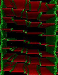 |
| Since 2004, materials scientists and nanotechnologists have been excited about a special of arrangement of atoms called a "coherent twin boundary" that can add strength and other advantages to metals like gold and copper. The CTB's are often described as "perfect," appearing like a one-atom-thick perfectly-flat plane in models and images. New research at the University of Vermont and Lawrence Livermore National Laboratory shows that these boundaries are not so perfect after all. Even more surprising, the newly discovered kinks and defects appear to be the cause of the CTB's strength.This image shows a simulation of atoms in a coherent twin boundary (shown in red) in copper. The newly discovered "kink" defects appear as green step-like structures and folds in the red areas. The red twin boundaries extend between columns of green atoms which represent grain boundaries within the copper.
Credit: Frederic Sansoz, University of Vermont |
Abstract:
One of the basic principles of nanotechnology is that when you make things extremely small—one nanometer is about five atoms wide, 100,000 times smaller than the diameter of a human hair—they are going to become more perfect.
Kinks and curves at the nanoscale: New research shows 'perfect twin boundaries' are not so perfect
Burlington, VT | Posted on May 20th, 2013"Perfect in the sense that their arrangement of atoms in the real world will become more like an idealized model," says University of Vermont engineer Frederic Sansoz, "with smaller crystals—in for example, gold or copper—it's easier to have fewer defects in them."
And eliminating the defects at the interface separating two crystals, or grains, has been shown by nanotechnology experts to be a powerful strategy for making materials stronger, more easily molded, and less electrically resistant—or a host of other qualities sought by designers and manufacturers.
Since 2004, when a seminal paper came out in Science, materials scientists have been excited about one special of arrangement of atoms in metals and other materials called a "coherent twin boundary" or CTB.
Based on theory and experiment, these coherent twin boundaries are often described as "perfect," appearing like a perfectly flat, one-atom-thick plane in computer models and electron microscope images.
Over the last decade, a body of literature has shown these coherent twin boundaries—found at the nanoscale within the crystalline structure of common metals like gold, silver and copper—are highly effective at making materials much stronger while maintaining their ability to undergo permanent change in shape without breaking and still allowing easy transmission of electrons—an important fact for computer manufacturing and other electronics applications.
But new research now shows that coherent twin boundaries are not so perfect after all.
A team of scientists, including Sansoz, a professor in UVM's College of Engineering and Mathematical Sciences, and colleagues from the Lawrence Livermore National Laboratory and elsewhere, write in the May 19 edition of Nature Materials that coherent twin boundaries found in copper "are inherently defective."
With a high-resolution electron microscope, using a more powerful technique than has ever been used to examine these boundaries, they found tiny kink-like steps and curvatures in what had previously been observed as perfect.
Even more surprising, these kinks and other defects appear to be the cause of the coherent twin boundary's strength and other desirable qualities.
"Everything we have learned on these materials in the past 10 years will have to be revisited with this new information," Sansoz says
The experiment, led by Morris Wang at the Lawrence Livermore Lab, applied a newly developed mapping technique to study the crystal orientation of CTBs in so-called nanotwinned copper and "boom—it revealed these defects," says Sansoz.
This real-world discovery conformed to earlier intriguing theoretical findings that Sansoz had been making with "atomistic simulations" on a computer. The lab results sent Sansoz back to his computer models where he introduced the newly discovered "kink" defects into his calculations. Using UVM's Vermont Advanced Computing Center, he theoretically confirmed that the kink defects observed by the Livermore team lead to "rather rich deformation processes at the atomic scale," he says, that do not exist with perfect twin boundaries.
With the computer model, "we found a series of completely new mechanisms," he says, for explaining why coherent twin boundaries simultaneously add strength and yet also allow stretching (what scientists call "tensile ductility")— properties that are usually mutually exclusive in conventional materials.
"We had no idea such defects existed," says Sansoz. "So much for the perfect twin boundary. We now call them defective twin boundaries."
For several decades, scientists have looked for ways to shrink the size of individual crystalline grains within metals and other materials. Like a series of dykes or walls within the larger structure, the boundaries between grains can slow internal slip and help resist failure. Generally, the more of these boundaries—the stronger the material.
Originally, scientists believed that coherent twin boundaries in materials were much more reliable and stable than conventional grain boundaries, which are incoherently full of defects. But the new research shows they could both contain similar types of defects despite very different boundary energies.
"Understanding these defective structures is the first step to take full use of these CTBs for strengthening and maintaining the ductility and electrical conductivity of many materials," Morris Wang said. "To understand the behavior and mechanisms of these defects will help our engineering design of these materials for high-strength applications."
For Sansoz, this discovery underlines a deep principle, "There are all manner of defects in nature," he says, "with nanotech, you are trying to control the way they are formed and dispersed in matter, and to understand their impact on properties. The point of this paper is that some defects make a material stronger."
####
For more information, please click here
Contacts:
Joshua Brown
802-656-3039
Copyright © University of Vermont
If you have a comment, please Contact us.Issuers of news releases, not 7th Wave, Inc. or Nanotechnology Now, are solely responsible for the accuracy of the content.
Bookmark:


| Related News Press |
News and information
![]() Quantum computer improves AI predictions April 17th, 2026
Quantum computer improves AI predictions April 17th, 2026
![]() Flexible sensor gains sensitivity under pressure April 17th, 2026
Flexible sensor gains sensitivity under pressure April 17th, 2026
![]() A reusable chip for particulate matter sensing April 17th, 2026
A reusable chip for particulate matter sensing April 17th, 2026
![]() Detecting vibrational quantum beating in the predissociation dynamics of SF6 using time-resolved photoelectron spectroscopy April 17th, 2026
Detecting vibrational quantum beating in the predissociation dynamics of SF6 using time-resolved photoelectron spectroscopy April 17th, 2026
Imaging
![]() Simple algorithm paired with standard imaging tool could predict failure in lithium metal batteries August 8th, 2025
Simple algorithm paired with standard imaging tool could predict failure in lithium metal batteries August 8th, 2025
![]() First real-time observation of two-dimensional melting process: Researchers at Mainz University unveil new insights into magnetic vortex structures August 8th, 2025
First real-time observation of two-dimensional melting process: Researchers at Mainz University unveil new insights into magnetic vortex structures August 8th, 2025
![]() New imaging approach transforms study of bacterial biofilms August 8th, 2025
New imaging approach transforms study of bacterial biofilms August 8th, 2025
Physics
![]() UC Irvine physicists discover method to reverse ‘quantum scrambling’ : The work addresses the problem of information loss in quantum computing system April 17th, 2026
UC Irvine physicists discover method to reverse ‘quantum scrambling’ : The work addresses the problem of information loss in quantum computing system April 17th, 2026
Laboratories
![]() Researchers develop molecular qubits that communicate at telecom frequencies October 3rd, 2025
Researchers develop molecular qubits that communicate at telecom frequencies October 3rd, 2025
Govt.-Legislation/Regulation/Funding/Policy
![]() Quantum computer improves AI predictions April 17th, 2026
Quantum computer improves AI predictions April 17th, 2026
![]() Metasurfaces smooth light to boost magnetic sensing precision January 30th, 2026
Metasurfaces smooth light to boost magnetic sensing precision January 30th, 2026
![]() New imaging approach transforms study of bacterial biofilms August 8th, 2025
New imaging approach transforms study of bacterial biofilms August 8th, 2025
Discoveries
![]() Quantum computer improves AI predictions April 17th, 2026
Quantum computer improves AI predictions April 17th, 2026
![]() Flexible sensor gains sensitivity under pressure April 17th, 2026
Flexible sensor gains sensitivity under pressure April 17th, 2026
![]() A reusable chip for particulate matter sensing April 17th, 2026
A reusable chip for particulate matter sensing April 17th, 2026
![]() Detecting vibrational quantum beating in the predissociation dynamics of SF6 using time-resolved photoelectron spectroscopy April 17th, 2026
Detecting vibrational quantum beating in the predissociation dynamics of SF6 using time-resolved photoelectron spectroscopy April 17th, 2026
Materials/Metamaterials/Magnetoresistance
![]() First real-time observation of two-dimensional melting process: Researchers at Mainz University unveil new insights into magnetic vortex structures August 8th, 2025
First real-time observation of two-dimensional melting process: Researchers at Mainz University unveil new insights into magnetic vortex structures August 8th, 2025
![]() Researchers unveil a groundbreaking clay-based solution to capture carbon dioxide and combat climate change June 6th, 2025
Researchers unveil a groundbreaking clay-based solution to capture carbon dioxide and combat climate change June 6th, 2025
![]() A 1960s idea inspires NBI researchers to study hitherto inaccessible quantum states June 6th, 2025
A 1960s idea inspires NBI researchers to study hitherto inaccessible quantum states June 6th, 2025
![]() Institute for Nanoscience hosts annual proposal planning meeting May 16th, 2025
Institute for Nanoscience hosts annual proposal planning meeting May 16th, 2025
Announcements
![]() A fundamentally new therapeutic approach to cystic fibrosis: Nanobody repairs cellular defect April 17th, 2026
A fundamentally new therapeutic approach to cystic fibrosis: Nanobody repairs cellular defect April 17th, 2026
![]() UC Irvine physicists discover method to reverse ‘quantum scrambling’ : The work addresses the problem of information loss in quantum computing system April 17th, 2026
UC Irvine physicists discover method to reverse ‘quantum scrambling’ : The work addresses the problem of information loss in quantum computing system April 17th, 2026
Tools
![]() Metasurfaces smooth light to boost magnetic sensing precision January 30th, 2026
Metasurfaces smooth light to boost magnetic sensing precision January 30th, 2026
![]() From sensors to smart systems: the rise of AI-driven photonic noses January 30th, 2026
From sensors to smart systems: the rise of AI-driven photonic noses January 30th, 2026
![]() Japan launches fully domestically produced quantum computer: Expo visitors to experience quantum computing firsthand August 8th, 2025
Japan launches fully domestically produced quantum computer: Expo visitors to experience quantum computing firsthand August 8th, 2025
Research partnerships
![]() Lab to industry: InSe wafer-scale breakthrough for future electronics August 8th, 2025
Lab to industry: InSe wafer-scale breakthrough for future electronics August 8th, 2025
![]() HKU physicists uncover hidden order in the quantum world through deconfined quantum critical points April 25th, 2025
HKU physicists uncover hidden order in the quantum world through deconfined quantum critical points April 25th, 2025
|
|
||
|
|
||
| The latest news from around the world, FREE | ||
|
|
||
|
|
||
| Premium Products | ||
|
|
||
|
Only the news you want to read!
Learn More |
||
|
|
||
|
Full-service, expert consulting
Learn More |
||
|
|
||