Home > Press > 'Super-resolution' microscope possible for nanostructures
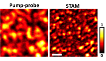 |
| A new type of super-resolution optical microscopy takes a high-resolution image (at right) of graphite "nanoplatelets" about 100 nanometers wide. The imaging system, called saturated transient absorption microscopy, or STAM, uses a trio of laser beams and represents a practical tool for biomedical and nanotechnology research. Weldon School of Biomedical Engineering, Purdue University |
Abstract:
Far-Field Imaging of Non-Fluorescent Species with Sub-Diffraction Resolution
Pu Wang1, #, Mikhail N. Slipchenko1, #, James Mitchell2, Chen Yang3, Eric O. Potma4, Xianfan Xu2, Ji-Xin Cheng13, *4
1 Weldon School of Biomedical Engineering, Purdue University
2 School of Mechanical Engineering and Birck Nanotechnology Center, Purdue University
3 Department of Chemistry, Purdue University
4 Department of Chemistry, University of California, Irvine
Super-resolution optical microscopy is opening a new window to unveil the unseen details on the nanoscopic scale. Current far-field super-resolution techniques rely on fluorescence as the read-out. Here, we demonstrate a scheme for breaking the diffraction limit in far-field imaging of non-fluorescent species by using spatially controlled saturation of electronic absorption. Our method is based on a pump-probe process where a modulated pump field perturbs the charge-carrier density in a sample, thus modulating the transmission of a probe field. A doughnut shape laser beam is then added to transiently saturate the electronic transition in the periphery of the focal volume, thus the induced modulation in the sequential probe pulse only occurs at the focal center. By raster scanning the three collinearly aligned beams, high-speed sub-diffraction-limited imaging of graphite nano-platelets was performed. This technique potentially enables super-resolution imaging of nano-materials and non-fluorescent chromophores, which may remain out of reach for fluorescence-based methods.
'Super-resolution' microscope possible for nanostructures
West Lafayette, IN | Posted on April 29th, 2013Researchers have found a way to see synthetic nanostructures and molecules using a new type of super-resolution optical microscopy that does not require fluorescent dyes, representing a practical tool for biomedical and nanotechnology research.
"Super-resolution optical microscopy has opened a new window into the nanoscopic world," said Ji-Xin Cheng, an associate professor of biomedical engineering and chemistry at Purdue University.
Conventional optical microscopes can resolve objects no smaller than about 300 nanometers, or billionths of a meter, a restriction known as the "diffraction limit," which is defined as half the width of the wavelength of light being used to view the specimen. However, researchers want to view molecules such as proteins and lipids, as well as synthetic nanostructures like nanotubes, which are a few nanometers in diameter.
Such a capability could bring advances in a diverse range of disciplines, from medicine to nanoelectronics, Cheng said.
"The diffraction limit represents the fundamental limit of optical imaging resolution," Cheng said. "Stefan Hell at the Max Planck Institute and others have developed super-resolution imaging methods that require fluorescent labels. Here, we demonstrate a new scheme for breaking the diffraction limit in optical imaging of non-fluorescent species. Because it is label-free, the signal is directly from the object so that we can learn more about the nanostructure."
Findings are detailed in a research paper that appeared online Sunday (April 28) in the journal Nature Photonics.
The imaging system, called saturated transient absorption microscopy, or STAM, uses a trio of laser beams, including a doughnut-shaped laser beam that selectively illuminates some molecules but not others. Electrons in the atoms of illuminated molecules are kicked temporarily into a higher energy level and are said to be excited, while the others remain in their "ground state." Images are generated using a laser called a probe to compare the contrast between the excited and ground-state molecules.
The researchers demonstrated the technique, taking images of graphite "nanoplatelets" about 100 nanometers wide.
"It's a proof of concept and has great potential for the study of nanomaterials, both natural and synthetic," Cheng said.
The doughnut-shaped laser excitation technique, invented by researcher Stefan Hell, makes it possible to focus on yet smaller objects. Researchers hope to improve the imaging system to see objects about 10 nanometers in diameter, or about 30 times smaller than possible using conventional optical microscopes.
"We are not there yet, but a few schemes can be applied to further increase the resolution of our system," Cheng said.
The paper was co-authored by biomedical engineering doctoral student Pu Wang; research scientist Mikhail N. Slipchenko; mechanical engineering doctoral student James Mitchell; Chen Yang, an assistant professor of physical chemistry at Purdue; Eric O. Potma, an associate professor of chemistry at the University of California, Irvine; Xianfan Xu, Purdue's James J. and Carol L. Shuttleworth Professor of Mechanical Engineering; and Cheng.
Future research may include work to use lasers with shorter wavelengths of light. Because the wavelengths are shorter, the doughnut hole is smaller, possibly allowing researchers to focus on smaller objects.
The work will be discussed during the third annual Spectroscopic Imaging: A New Window into the Unseen World workshop on May 23 and 24 at Purdue. The workshop is hosted by the university's Weldon School of Biomedical Engineering. More workshop information is available at www.conf.purdue.edu/cheng
The research is funded by the National Institutes of Health, National Science Foundation and the Defense Advanced Research Projects Agency.
Note to Journalists: Ji-Xin Cheng's name is pronounced "Gee-Shin." Journalists may obtain a copy of the research paper by contacting Nature at or calling 212-726-9231.
####
For more information, please click here
Contacts:
Writer:
Emil Venere
765-494-4709
Sources:
Ji-Xin Cheng
765-494-4335
Chen Yang
765-496-3346
Copyright © Purdue University
If you have a comment, please Contact us.Issuers of news releases, not 7th Wave, Inc. or Nanotechnology Now, are solely responsible for the accuracy of the content.
Bookmark:


| Related Links |
| Related News Press |
News and information
![]() Quantum computer improves AI predictions April 17th, 2026
Quantum computer improves AI predictions April 17th, 2026
![]() Flexible sensor gains sensitivity under pressure April 17th, 2026
Flexible sensor gains sensitivity under pressure April 17th, 2026
![]() A reusable chip for particulate matter sensing April 17th, 2026
A reusable chip for particulate matter sensing April 17th, 2026
![]() Detecting vibrational quantum beating in the predissociation dynamics of SF6 using time-resolved photoelectron spectroscopy April 17th, 2026
Detecting vibrational quantum beating in the predissociation dynamics of SF6 using time-resolved photoelectron spectroscopy April 17th, 2026
Imaging
![]() Simple algorithm paired with standard imaging tool could predict failure in lithium metal batteries August 8th, 2025
Simple algorithm paired with standard imaging tool could predict failure in lithium metal batteries August 8th, 2025
Govt.-Legislation/Regulation/Funding/Policy
![]() Quantum computer improves AI predictions April 17th, 2026
Quantum computer improves AI predictions April 17th, 2026
![]() Metasurfaces smooth light to boost magnetic sensing precision January 30th, 2026
Metasurfaces smooth light to boost magnetic sensing precision January 30th, 2026
![]() New imaging approach transforms study of bacterial biofilms August 8th, 2025
New imaging approach transforms study of bacterial biofilms August 8th, 2025
Discoveries
![]() Quantum computer improves AI predictions April 17th, 2026
Quantum computer improves AI predictions April 17th, 2026
![]() Flexible sensor gains sensitivity under pressure April 17th, 2026
Flexible sensor gains sensitivity under pressure April 17th, 2026
![]() A reusable chip for particulate matter sensing April 17th, 2026
A reusable chip for particulate matter sensing April 17th, 2026
![]() Detecting vibrational quantum beating in the predissociation dynamics of SF6 using time-resolved photoelectron spectroscopy April 17th, 2026
Detecting vibrational quantum beating in the predissociation dynamics of SF6 using time-resolved photoelectron spectroscopy April 17th, 2026
Announcements
![]() A fundamentally new therapeutic approach to cystic fibrosis: Nanobody repairs cellular defect April 17th, 2026
A fundamentally new therapeutic approach to cystic fibrosis: Nanobody repairs cellular defect April 17th, 2026
![]() UC Irvine physicists discover method to reverse �quantum scrambling� : The work addresses the problem of information loss in quantum computing system April 17th, 2026
UC Irvine physicists discover method to reverse �quantum scrambling� : The work addresses the problem of information loss in quantum computing system April 17th, 2026
Tools
![]() Metasurfaces smooth light to boost magnetic sensing precision January 30th, 2026
Metasurfaces smooth light to boost magnetic sensing precision January 30th, 2026
![]() From sensors to smart systems: the rise of AI-driven photonic noses January 30th, 2026
From sensors to smart systems: the rise of AI-driven photonic noses January 30th, 2026
![]() Japan launches fully domestically produced quantum computer: Expo visitors to experience quantum computing firsthand August 8th, 2025
Japan launches fully domestically produced quantum computer: Expo visitors to experience quantum computing firsthand August 8th, 2025
Military
![]() Quantum engineers �squeeze� laser frequency combs to make more sensitive gas sensors January 17th, 2025
Quantum engineers �squeeze� laser frequency combs to make more sensitive gas sensors January 17th, 2025
![]() Chainmail-like material could be the future of armor: First 2D mechanically interlocked polymer exhibits exceptional flexibility and strength January 17th, 2025
Chainmail-like material could be the future of armor: First 2D mechanically interlocked polymer exhibits exceptional flexibility and strength January 17th, 2025
![]() Single atoms show their true color July 5th, 2024
Single atoms show their true color July 5th, 2024
![]() NRL charters Navy�s quantum inertial navigation path to reduce drift April 5th, 2024
NRL charters Navy�s quantum inertial navigation path to reduce drift April 5th, 2024
Photonics/Optics/Lasers
![]() Metasurfaces smooth light to boost magnetic sensing precision January 30th, 2026
Metasurfaces smooth light to boost magnetic sensing precision January 30th, 2026
![]() From sensors to smart systems: the rise of AI-driven photonic noses January 30th, 2026
From sensors to smart systems: the rise of AI-driven photonic noses January 30th, 2026
|
|
||
|
|
||
| The latest news from around the world, FREE | ||
|
|
||
|
|
||
| Premium Products | ||
|
|
||
|
Only the news you want to read!
Learn More |
||
|
|
||
|
Full-service, expert consulting
Learn More |
||
|
|
||