Home > Press > High-performance, NW-OPTs open the way for optoelectronic device miniaturization
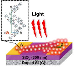 |
| Schematic diagram of single-crystalline nanowire organic phototransistors
Copyright @ Wiley-VCH Verlag GmbH & Co. KGaA. |
Abstract:
Research team of Ulsan National Institute of Science and Technology (UNIST), Ulsan, South Korea, developed high-performance organic phototransistors (OPTs) based on single-crystalline n-channel organic nanowires.
High-performance, NW-OPTs open the way for optoelectronic device miniaturization
Ulsan, Republic of Korea | Posted on March 12th, 2013 Phototransistors are a kind of transistors in which the incident light intensity can modulate the charge-carrier density in the channel. Compared with conventional photodiodes, phototransistors enable easier control of light-detection sensitivity without problems such as the noise increment. However, to date, the research has mostly focused on thin-film OPTs, and nanoscale OPTs have scarcely been reported.
OPTs have many intrinsic advantages over their inorganic counterparts, such as the chemical tunability of optoelectronic properties by molecular design and high potential in low cost, light-weight, flexible applications.
Single-crystalline nano-/microwires (NWs/MWs) based on organic semiconductors have attracted great interest recently as they are promising building blocks for various electronic and optoelectronic applications. In particular, OPTs based on single-crystalline NWs/MWs may yield higher light sensitivity than their bulk counterparts. In addition, their one-dimensional, intrinsically defect-free and highly ordered nature will allow a deeper understanding of the fundamental mechanisms of charge generation and transport in OPTs, while enabling a bottom-up fabrication of optoelectronic nanodevices.
Prof. Joon Hak Oh and Hojeong Yu, working at UNIST, together with Prof. Zhenan Bao at Stanford University, USA, have worked on n-channel single-crystalline nanowire organic phototransistors (NW-OPTs) and observed significant enhancement in the charge-carrier mobility of NW-OPTs.
Prof. Oh said, "The development of OPTs based on n-channel single-crystalline organic semiconducting NWs/MWs is highly desirable for the bottom-up fabrication of complementary metal oxide semiconductor (CMOS)-like photoelectronic circuits, which provides various advantages such as high operational stability, easy control of photoswitching voltages, high photosensitivity and responsivity."
The photoelectronic characteristics of the single-crystalline NW-OPTs such as the photoresponsivity, the photo-switching ratio, and the photoconductive gain, were analyzed from the I-V characteristics coupled with light irradiation and compared with those of vacuum-deposited thin-film devices. The external quantum efficiencies (EQEs) were also investigated for the NW-OPTs and thin-film OPTs. In addition, they calculated the charge accumulation and release rates from deep traps, and investigated the effects of incident light intensity on their photoelectronic properties.
A mobility enhancement is observed when the incident optical power density increases and the wavelength of the light source matches the light-absorption range of the photoactive material. The photoswitching ratio is strongly dependent upon the incident optical power density, whereas the photoresponsivity is more dependent on matching the light-source wavelength with the maximum absorption range of the photoactive material.
NW-OPTs based on n-channel semiconductor, N,N ′-bis(2-phenylethyl)-perylene-3,4:9,10-tetracarboxylic diimide (BPE-PTCDI), exhibited much higher external quantum efficiency (EQE) values (≈7900 times larger) than thin-film OPTs, with a maximum EQE of 263 000%. This phenomena result from the intrinsically defect-free single-crystalline nature of the BPE-PTCDI NWs. In addition, an approach was devised to analyze the charge-transport behaviors using charge accumulation/release rates from deep traps under on/off switching of external light sources.
"Our approach to charge-accumulation/release-rate calculations could provide a fundamental understanding about charge-carrier-density variations under light irradiation, which subsequently enables in-depth study of OPTs," said Prof. Oh, "Hence organic single-crystalline NW-OPTs are a highly promising alternative to conventional thin-film-type photodiodes, and can effectively pave the way for optoelectronic device miniaturization."
This research was supported by a National Research Foundation of Korea (NRF) Grant funded by the Ministry of Education, Science, and Technology (MEST), and the Global Frontier Research Center for Advanced Soft Electronics and published in Advanced Functional Materials (Title: High-Performance Phototransistors Based on Single-Crystalline n-Channel Organic Nanowires and Photogenerated Charge-Carrier Behaviors, 5 Feb 2013).
####
For more information, please click here
Contacts:
Eunhee Song
82-522-171-224
Copyright © Ulsan National Institute of Science and Technology
If you have a comment, please Contact us.Issuers of news releases, not 7th Wave, Inc. or Nanotechnology Now, are solely responsible for the accuracy of the content.
Bookmark:


| Related Links |
| Related News Press |
News and information
![]() Quantum computer improves AI predictions April 17th, 2026
Quantum computer improves AI predictions April 17th, 2026
![]() Flexible sensor gains sensitivity under pressure April 17th, 2026
Flexible sensor gains sensitivity under pressure April 17th, 2026
![]() A reusable chip for particulate matter sensing April 17th, 2026
A reusable chip for particulate matter sensing April 17th, 2026
![]() Detecting vibrational quantum beating in the predissociation dynamics of SF6 using time-resolved photoelectron spectroscopy April 17th, 2026
Detecting vibrational quantum beating in the predissociation dynamics of SF6 using time-resolved photoelectron spectroscopy April 17th, 2026
Govt.-Legislation/Regulation/Funding/Policy
![]() Quantum computer improves AI predictions April 17th, 2026
Quantum computer improves AI predictions April 17th, 2026
![]() Metasurfaces smooth light to boost magnetic sensing precision January 30th, 2026
Metasurfaces smooth light to boost magnetic sensing precision January 30th, 2026
![]() New imaging approach transforms study of bacterial biofilms August 8th, 2025
New imaging approach transforms study of bacterial biofilms August 8th, 2025
Chip Technology
![]() A reusable chip for particulate matter sensing April 17th, 2026
A reusable chip for particulate matter sensing April 17th, 2026
![]() Metasurfaces smooth light to boost magnetic sensing precision January 30th, 2026
Metasurfaces smooth light to boost magnetic sensing precision January 30th, 2026
Discoveries
![]() Quantum computer improves AI predictions April 17th, 2026
Quantum computer improves AI predictions April 17th, 2026
![]() Flexible sensor gains sensitivity under pressure April 17th, 2026
Flexible sensor gains sensitivity under pressure April 17th, 2026
![]() A reusable chip for particulate matter sensing April 17th, 2026
A reusable chip for particulate matter sensing April 17th, 2026
![]() Detecting vibrational quantum beating in the predissociation dynamics of SF6 using time-resolved photoelectron spectroscopy April 17th, 2026
Detecting vibrational quantum beating in the predissociation dynamics of SF6 using time-resolved photoelectron spectroscopy April 17th, 2026
Announcements
![]() A fundamentally new therapeutic approach to cystic fibrosis: Nanobody repairs cellular defect April 17th, 2026
A fundamentally new therapeutic approach to cystic fibrosis: Nanobody repairs cellular defect April 17th, 2026
![]() UC Irvine physicists discover method to reverse �quantum scrambling� : The work addresses the problem of information loss in quantum computing system April 17th, 2026
UC Irvine physicists discover method to reverse �quantum scrambling� : The work addresses the problem of information loss in quantum computing system April 17th, 2026
Photonics/Optics/Lasers
![]() Metasurfaces smooth light to boost magnetic sensing precision January 30th, 2026
Metasurfaces smooth light to boost magnetic sensing precision January 30th, 2026
![]() From sensors to smart systems: the rise of AI-driven photonic noses January 30th, 2026
From sensors to smart systems: the rise of AI-driven photonic noses January 30th, 2026
Research partnerships
![]() Lab to industry: InSe wafer-scale breakthrough for future electronics August 8th, 2025
Lab to industry: InSe wafer-scale breakthrough for future electronics August 8th, 2025
![]() HKU physicists uncover hidden order in the quantum world through deconfined quantum critical points April 25th, 2025
HKU physicists uncover hidden order in the quantum world through deconfined quantum critical points April 25th, 2025
|
|
||
|
|
||
| The latest news from around the world, FREE | ||
|
|
||
|
|
||
| Premium Products | ||
|
|
||
|
Only the news you want to read!
Learn More |
||
|
|
||
|
Full-service, expert consulting
Learn More |
||
|
|
||