Home > Press > CRAIC Technologies Raman Spectral Surface Mapping™ Capability
 |
Abstract:
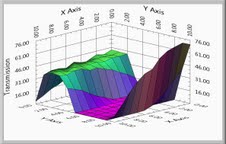
CRAIC Technologies introduces Spectral Surface Mapping™ which allows automatic Raman spectral mapping with microscopic spatial resolution. 3D maps can be generated for Raman spectra quickly, easily and automatically.
CRAIC Technologies Raman Spectral Surface Mapping™ Capability
San Dimas, CA | Posted on February 2nd, 2013CRAIC Technologies, the world leading innovator of microanalysis solutions, is proud to announce Raman Spectral Surface Mapping™ (S2M™) capabilities for its Apollo™ Raman microspectrometer line. S2M™ gives CRAIC Raman microspectrometer users the ability to map the Raman spectral variation of their samples with microscopic spatial resolution. Surface profiles can be created from Raman microspectral data from the CRAIC Apollo™ Raman microspectrometer. Apollo™ Raman microspectrometers can now created highly detailed spectral maps with micron scale resolution of Raman spectral features rapidly and automatically.
"CRAIC Technologies has worked to develop the Spectral Surface Mapping™ package because of customer requests. Adding Raman spectral mapping was an obvious step. Our customers wanted the ability to automatically survey and characterize the entire surface of samples by their Raman spectral characteristics. They also wanted a high spatial resolution" states Dr. Paul Martin, President of CRAIC Technologies. "S2M™ with the Apollo™ Raman microspectrometer does just that. It allows you to collect spectral data from thousands of points with a user defined mapping pattern. The user is then able to analyze the entire object by changes to its Raman spectral characteristics. The user can also pull up the full spectrum for each point."
Spectral Surface Mapping™ includes a software module to be used with CRAIC Technologies MINERVA-Raman™ microspectrometer control software. When employed with CRAIC Technologies Apollo™ Raman microspectrometers with programmable stages, S2M™ allows a user to automatically take spectral measurements with user-defined mapping patterns that reach to the limits of the stage itself. With the ability to measure up to a million points, high definition maps of the Raman spectral response of the sample may be generated. And because of the flexibility and power of the software, Raman spectral responses may even be collected and mapped when used with CRAIC Technologies Apollo™ Raman microspectrometers. S2M™ gives even more power to the scientist and engineer to study the entire surface of their samples at the highest level of detail.
####
About CRAIC Technologies, Inc.
CRAIC Technologies, Inc. is a global technology leader focused on innovations for microscopy and microspectroscopy in the ultraviolet, visible and near-infrared regions. CRAIC Technologies creates cutting-edge solutions, with the very best in customer support, by listening to our customers and implementing solutions that integrate operational excellence and technology expertise. CRAIC Technologies provides answers for customers in forensic sciences, biotechnology, semiconductor, geology, nanotechnology and materials science markets who demand quality, accuracy, precision, speed and the best in customer support.
For more information, please click here
Contacts:
CRAIC Technologies, Inc.
www.microspectra.com/
+1-310-573-8180
Copyright © CRAIC Technologies, Inc.
If you have a comment, please Contact us.Issuers of news releases, not 7th Wave, Inc. or Nanotechnology Now, are solely responsible for the accuracy of the content.
| Related News Press |
News and information
![]() Quantum computer improves AI predictions April 17th, 2026
Quantum computer improves AI predictions April 17th, 2026
![]() Flexible sensor gains sensitivity under pressure April 17th, 2026
Flexible sensor gains sensitivity under pressure April 17th, 2026
![]() A reusable chip for particulate matter sensing April 17th, 2026
A reusable chip for particulate matter sensing April 17th, 2026
![]() Detecting vibrational quantum beating in the predissociation dynamics of SF6 using time-resolved photoelectron spectroscopy April 17th, 2026
Detecting vibrational quantum beating in the predissociation dynamics of SF6 using time-resolved photoelectron spectroscopy April 17th, 2026
Imaging
![]() Simple algorithm paired with standard imaging tool could predict failure in lithium metal batteries August 8th, 2025
Simple algorithm paired with standard imaging tool could predict failure in lithium metal batteries August 8th, 2025
Announcements
![]() A fundamentally new therapeutic approach to cystic fibrosis: Nanobody repairs cellular defect April 17th, 2026
A fundamentally new therapeutic approach to cystic fibrosis: Nanobody repairs cellular defect April 17th, 2026
![]() UC Irvine physicists discover method to reverse ‘quantum scrambling’ : The work addresses the problem of information loss in quantum computing system April 17th, 2026
UC Irvine physicists discover method to reverse ‘quantum scrambling’ : The work addresses the problem of information loss in quantum computing system April 17th, 2026
Tools
![]() Metasurfaces smooth light to boost magnetic sensing precision January 30th, 2026
Metasurfaces smooth light to boost magnetic sensing precision January 30th, 2026
![]() From sensors to smart systems: the rise of AI-driven photonic noses January 30th, 2026
From sensors to smart systems: the rise of AI-driven photonic noses January 30th, 2026
![]() Japan launches fully domestically produced quantum computer: Expo visitors to experience quantum computing firsthand August 8th, 2025
Japan launches fully domestically produced quantum computer: Expo visitors to experience quantum computing firsthand August 8th, 2025
|
|
||
|
|
||
| The latest news from around the world, FREE | ||
|
|
||
|
|
||
| Premium Products | ||
|
|
||
|
Only the news you want to read!
Learn More |
||
|
|
||
|
Full-service, expert consulting
Learn More |
||
|
|
||


