Home > Press > Imec Shows Path Toward Non-Si Devices at IEDM 2012
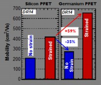 |
| Comparison of mobility in unstrained and strained Si and Ge p-FinFETs. Unstrained Ge shows degraded mobility w.r.t. strained Si. Strained Ge can improve pFET mobility by 59% |
Abstract:
At this week's IEEE International Electron Devices Meeting (IEDM 2012), imec addressed key challenges of scaling beyond silicon-channel finFETs. Imec showed that channel mobility can be boosted by growing non-Si channels on a strain relaxed buffer (SRB), and demonstrated excellent scalability potential of the technology. Moreover, imec revealed insight on the unique influence oxide trapping has on the gate stack mobility in High-Mobility Ge and III-V channels.
Imec Shows Path Toward Non-Si Devices at IEDM 2012
San Francisco, CA | Posted on December 11th, 2012For logic device technology, the industry previously used SiGe source/drain stressors to enhance the Si channel mobility. However, this process is reaching its scalability limits due to lay-out dependent defects. At IEDM 2012, imec demonstrated excellent scalability toward the 1nm/10nm and 7nm nodes with Ge-channel FinFETs through a Si fin replacement process. Imec also delivered significant mobility boosts (of at least 50 percent) when growing a Ge channel on a SiGe 75 percent localized strain relaxed buffer, compared to strained Si channels (*).
Whereas recent work resulted in the reduction of the density of oxide-semiconductor interface traps of III-V and Ge MOS devices, imec presented new evidence of additional trapping of carriers, namely in the gate dielectrics of these non-Si devices. For the first time, imec showed the adverse impact of such oxide border traps on device performance. Imec's research revealed that near-interface (fast) oxide traps can be probed using the AC-gm (AC transconductance) technique. Shallow (fast) oxide traps are believed to be responsible for non-Si MOSFET on-state frequency-dependent transconductance. This, in violation of the frequency invariance pre-requisite, can post a significant problem at circuit level. Imec also mapped out the slow border traps in the high-k dielectrics using the TSCIS (Trap Spectroscopy by Charge Injection and Sensing) technique. Imec demonstrated the charging of slower traps in the high-k dielectric, resulting in a drifting threshold voltage. As a result, a very low overdrive voltage is predicted (Ge/212mV, InGaAs/255mV, ~1/3 of the ITRS spec on Si) for the 10 year-lifetime of devices. Charge interaction with oxide border traps remains a challenge when moving toward non-Si devices.
"With each new technology generation, challenges are immense. And imec has always come up with solutions to extend Moore's law," stated Aaron Thean, director logic program at imec. "Moving on towards the 14nm node and beyond, we are confident that again, we will find solutions for the challenges that lie ahead. We are looking into high-mobility channel materials, such as Ge and III/V compounds, focusing on two main challenges namely how to implement non-Si materials into the device architecture and how to overcome some of the fundamental physics of the gate stack related to passivation."
These results were obtained in cooperation with imec's key partners in its core CMOS programs: Globalfoundries, INTEL, Micron, Panasonic, Samsung, TSMC, Elpida, SK Hynix, Fujitsu, Toshiba/Sandisk, and Sony.
####
About IMEC
Imec performs world-leading research in nanoelectronics. Imec leverages its scientific knowledge with the innovative power of its global partnerships in ICT, healthcare and energy. Imec delivers industry-relevant technology solutions. In a unique high-tech environment, its international top talent is committed to providing the building blocks for a better life in a sustainable society. Imec is headquartered in Leuven, Belgium, and has offices in Belgium, the Netherlands, Taiwan, US, China, India and Japan. Its staff of close to 2,000 people includes more than 600 industrial residents and guest researchers. In 2011, imec's revenue (P&L) was about 300 million euro. Further information on imec can be found at www.imec.be.
Imec is a registered trademark for the activities of IMEC International (a legal entity set up under Belgian law as a "stichting van openbaar nut�), imec Belgium (IMEC vzw supported by the Flemish Government), imec the Netherlands (Stichting IMEC Nederland, part of Holst Centre which is supported by the Dutch Government), imec Taiwan (IMEC Taiwan Co.) and imec China (IMEC Microelectronics (Shangai) Co. Ltd.) and imec India (Imec India Private Limited).
For more information, please click here
Copyright © IMEC
If you have a comment, please Contact us.Issuers of news releases, not 7th Wave, Inc. or Nanotechnology Now, are solely responsible for the accuracy of the content.
Bookmark:


| Related News Press |
News and information
![]() Quantum computer improves AI predictions April 17th, 2026
Quantum computer improves AI predictions April 17th, 2026
![]() Flexible sensor gains sensitivity under pressure April 17th, 2026
Flexible sensor gains sensitivity under pressure April 17th, 2026
![]() A reusable chip for particulate matter sensing April 17th, 2026
A reusable chip for particulate matter sensing April 17th, 2026
![]() Detecting vibrational quantum beating in the predissociation dynamics of SF6 using time-resolved photoelectron spectroscopy April 17th, 2026
Detecting vibrational quantum beating in the predissociation dynamics of SF6 using time-resolved photoelectron spectroscopy April 17th, 2026
Chip Technology
![]() A reusable chip for particulate matter sensing April 17th, 2026
A reusable chip for particulate matter sensing April 17th, 2026
![]() Metasurfaces smooth light to boost magnetic sensing precision January 30th, 2026
Metasurfaces smooth light to boost magnetic sensing precision January 30th, 2026
Announcements
![]() A fundamentally new therapeutic approach to cystic fibrosis: Nanobody repairs cellular defect April 17th, 2026
A fundamentally new therapeutic approach to cystic fibrosis: Nanobody repairs cellular defect April 17th, 2026
![]() UC Irvine physicists discover method to reverse �quantum scrambling� : The work addresses the problem of information loss in quantum computing system April 17th, 2026
UC Irvine physicists discover method to reverse �quantum scrambling� : The work addresses the problem of information loss in quantum computing system April 17th, 2026
Events/Classes
![]() Institute for Nanoscience hosts annual proposal planning meeting May 16th, 2025
Institute for Nanoscience hosts annual proposal planning meeting May 16th, 2025
![]() A New Blue: Mysterious origin of the ribbontail ray�s electric blue spots revealed July 5th, 2024
A New Blue: Mysterious origin of the ribbontail ray�s electric blue spots revealed July 5th, 2024
![]() Researchers demonstrate co-propagation of quantum and classical signals: Study shows that quantum encryption can be implemented in existing fiber networks January 20th, 2023
Researchers demonstrate co-propagation of quantum and classical signals: Study shows that quantum encryption can be implemented in existing fiber networks January 20th, 2023
Alliances/Trade associations/Partnerships/Distributorships
![]() Chicago Quantum Exchange welcomes six new partners highlighting quantum technology solutions, from Chicago and beyond September 23rd, 2022
Chicago Quantum Exchange welcomes six new partners highlighting quantum technology solutions, from Chicago and beyond September 23rd, 2022
![]() University of Illinois Chicago joins Brookhaven Lab's Quantum Center June 10th, 2022
University of Illinois Chicago joins Brookhaven Lab's Quantum Center June 10th, 2022
Research partnerships
![]() Lab to industry: InSe wafer-scale breakthrough for future electronics August 8th, 2025
Lab to industry: InSe wafer-scale breakthrough for future electronics August 8th, 2025
![]() HKU physicists uncover hidden order in the quantum world through deconfined quantum critical points April 25th, 2025
HKU physicists uncover hidden order in the quantum world through deconfined quantum critical points April 25th, 2025
|
|
||
|
|
||
| The latest news from around the world, FREE | ||
|
|
||
|
|
||
| Premium Products | ||
|
|
||
|
Only the news you want to read!
Learn More |
||
|
|
||
|
Full-service, expert consulting
Learn More |
||
|
|
||