Home > Press > Carl Zeiss introduces ORION NanoFab- Extending nanofabrication to the sub-10 nanometer scale (first multi-ion-beam tool based on Gas Field Ion Source (GFIS) technology)
 |
Abstract:
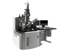
Carl Zeiss Microscopy is introducing ORION NanoFab at the European Microscopy Congress (EMC) in Manchester, UK. It is the first multi-ion-beam tool based on Gas Field Ion Source (GFIS) technology. As a major enhancement to the existing helium ion microscope, ORION NanoFab also utilizes neon ions. The system is therefore capable of providing a complete sub-10 nanometer nanofabrication and sub-nanometer imaging solution for industry, government, and academic research laboratories. An optional gallium focused ion beam (FIB) column can also be integrated.
Carl Zeiss introduces ORION NanoFab- Extending nanofabrication to the sub-10 nanometer scale (first multi-ion-beam tool based on Gas Field Ion Source (GFIS) technology)
Jena, Germany / Manchester, UK | Posted on November 28th, 2012"This instrument offers sub-nanometer spatial resolution coupled with an extremely high depth of field, for the study of a wide variety of materials such as carbon based materials, co-polymers, and device structures, and also offers options for a variety of advanced microanalytical techniques," says Dr. David Joy, Distinguished Scientist at the Center for Nanophase Materials Science (CNMS), Oak Ridge National Laboratory. CNMS at Oak Ridge National Laboratory (ORNL) is a Department of Energy / Office of Science Nanoscale Science Research Center (NSRC).
The neon ion beam offers precise machining and nanofabrication capabilities due to higher sputter yields in ion beam milling and faster resist exposure in ion beam lithography. The helium ion beam allows sub-10 nm nanofabrication as well as high resolution imaging capability in the same instrument. The optional state-of-the-art gallium FIB column allows massive material removal. This makes ORION NanoFab the most versatile nanofabrication and imaging platform available.
"I have finally found the system that I was looking for the past five years," says Dr. Qianjin Wang from the Physics Department at Nanjing University in China. "As a gallium FIB user for past ten years, I feel lucky that I will be at the forefront of revolution in the nanoworld as I focus on my research on optical properties of artificial nanoscale structures."
"We're very excited about all aspects of ORION NanoFab." says Michael Phaneuf, President of Fibics Incorporated, a FIB/SEM applications development company established in Ottawa, Canada in 1997. "The evolution to this generation helium-neon-gallium tool is truly impressive. The possibilities for multi-scale nanofabrication combining all three beams are truly remarkable, and the applications involving high resolution imaging with helium and neon are only now beginning to be realized. We are eager to start applications development on this platform, and see where it leads."
####
About Carl Zeiss Microscopy
Carl Zeiss Microscopy, LLC, offers microscopy solutions and systems for research, routine, and industrial applications. In addition, Carl Zeiss Microscopy markets microscopy systems for the clinical market, as well as optical sensor systems for industrial and pharmaceutical applications. Since 1846, Carl Zeiss has remained committed to enabling science and technology to go beyond what man can see. Today, Carl Zeiss is a global leader in the optical and opto-electronic industries.
With 12,872 current employees and offices in over 30 countries, Carl Zeiss is represented in more than 100 countries with production centers in Europe, North America, Central America and Asia. For more information on the breadth of solutions offered by Carl Zeiss Microscopy, please visit www.zeiss.com/micro.
For more information, please click here
Contacts:
Maya Everett
Carl Zeiss Microscopy
(914) 681-7782
Copyright © Carl Zeiss Microscopy, LLC
If you have a comment, please Contact us.Issuers of news releases, not 7th Wave, Inc. or Nanotechnology Now, are solely responsible for the accuracy of the content.
Bookmark:


| Related News Press |
News and information
![]() Quantum computer improves AI predictions April 17th, 2026
Quantum computer improves AI predictions April 17th, 2026
![]() Flexible sensor gains sensitivity under pressure April 17th, 2026
Flexible sensor gains sensitivity under pressure April 17th, 2026
![]() A reusable chip for particulate matter sensing April 17th, 2026
A reusable chip for particulate matter sensing April 17th, 2026
![]() Detecting vibrational quantum beating in the predissociation dynamics of SF6 using time-resolved photoelectron spectroscopy April 17th, 2026
Detecting vibrational quantum beating in the predissociation dynamics of SF6 using time-resolved photoelectron spectroscopy April 17th, 2026
Imaging
![]() Simple algorithm paired with standard imaging tool could predict failure in lithium metal batteries August 8th, 2025
Simple algorithm paired with standard imaging tool could predict failure in lithium metal batteries August 8th, 2025
Announcements
![]() A fundamentally new therapeutic approach to cystic fibrosis: Nanobody repairs cellular defect April 17th, 2026
A fundamentally new therapeutic approach to cystic fibrosis: Nanobody repairs cellular defect April 17th, 2026
![]() UC Irvine physicists discover method to reverse �quantum scrambling� : The work addresses the problem of information loss in quantum computing system April 17th, 2026
UC Irvine physicists discover method to reverse �quantum scrambling� : The work addresses the problem of information loss in quantum computing system April 17th, 2026
Tools
![]() Metasurfaces smooth light to boost magnetic sensing precision January 30th, 2026
Metasurfaces smooth light to boost magnetic sensing precision January 30th, 2026
![]() From sensors to smart systems: the rise of AI-driven photonic noses January 30th, 2026
From sensors to smart systems: the rise of AI-driven photonic noses January 30th, 2026
![]() Japan launches fully domestically produced quantum computer: Expo visitors to experience quantum computing firsthand August 8th, 2025
Japan launches fully domestically produced quantum computer: Expo visitors to experience quantum computing firsthand August 8th, 2025
|
|
||
|
|
||
| The latest news from around the world, FREE | ||
|
|
||
|
|
||
| Premium Products | ||
|
|
||
|
Only the news you want to read!
Learn More |
||
|
|
||
|
Full-service, expert consulting
Learn More |
||
|
|
||