Home > Press > Ultra fast optical amplifier: silicon and erbium on one chip for the first time
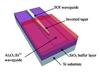 |
| Image of the chip including silicon optical waveguide (SOI: silicon on insulator) as well as erbium-doped aluminium oxyde. |
Abstract:
Within optical microchips, light finds its way through channels, waveguides, made of silicon. Light from a glass fiber, for example, is led through a structure of optical channels with splitters and couplers. Silicon is the workhorse for this, but it is still passive conduction of light, with some losses as well. To be able to amplify the signal, or even to include a light source on the chip, extra steps are necessary. Other types of semiconductors, like Gallium Arsenide, are an option. But materials doped with the rare earth material erbium have good amplification properties as well.
Ultra fast optical amplifier: silicon and erbium on one chip for the first time
Enschede, Netherlands | Posted on September 22nd, 2012Until now, no chip existed, on which both silicon and erbium-doped material were integrated. In her thesis, PhD candidate Laura Agazzi of the University of Twente demonstrates a working chip for the first time. It will be able to amplify light at speeds up to 170 Gbit/sec. The prototype chip has a signal gain of 7.2 decibel at infrared light (1533 nanometer).
The prototype is a starting point, but the results are very promising. One of the possibilities is a laser with an extremely narrow linewidth of 1.7 kHz. "In any application that needs emission or amplification of light, this integration of both materials is useful. It is not limited to telecom. You could use these chips for sensor purposes, for tracing extremely small particles, for example," Agazzi adds.
Trade-off
Laura Agazzi has investigated the optical properties of aluminium oxide doped with erbium, to understand the mechanisms that influence the amplification properties in a negative way. One of these is called energy-transfer up conversion (ETU), which is detrimental for good functionality."If you want a large amplification, you would like to put many erbium ions in the material, this in turn can cause a higher ETU. There are possibilities in adapting the host material, causing less interaction of the ions. With my models, I have gained better insight in these and other mechanisms that lower the amplification.
Laura Agazzi (1983, Vimercate, Italie) conducted her research within the Integrated Optical Microsystems (IOMS) of prof Markus Pollnau, which is part of the MESA+ Institute for Nanotechnology of the University of Twente. On Sep 20 she successfully defended her thesis Spectroscopic Excitation and Quenching Processes in Rare-Earth-Ion-Doped Al2O3 and their Impact on Amplifier and Laser Performance. Her thesis, or a summary, are available digitally.
####
For more information, please click here
Contacts:
Wiebe van der Veen
+31612185692
Copyright © AlphaGalileo
If you have a comment, please Contact us.Issuers of news releases, not 7th Wave, Inc. or Nanotechnology Now, are solely responsible for the accuracy of the content.
Bookmark:


| Related News Press |
News and information
![]() Quantum computer improves AI predictions April 17th, 2026
Quantum computer improves AI predictions April 17th, 2026
![]() Flexible sensor gains sensitivity under pressure April 17th, 2026
Flexible sensor gains sensitivity under pressure April 17th, 2026
![]() A reusable chip for particulate matter sensing April 17th, 2026
A reusable chip for particulate matter sensing April 17th, 2026
![]() Detecting vibrational quantum beating in the predissociation dynamics of SF6 using time-resolved photoelectron spectroscopy April 17th, 2026
Detecting vibrational quantum beating in the predissociation dynamics of SF6 using time-resolved photoelectron spectroscopy April 17th, 2026
Chip Technology
![]() A reusable chip for particulate matter sensing April 17th, 2026
A reusable chip for particulate matter sensing April 17th, 2026
![]() Metasurfaces smooth light to boost magnetic sensing precision January 30th, 2026
Metasurfaces smooth light to boost magnetic sensing precision January 30th, 2026
Optical computing/Photonic computing
![]() ICFO researchers overcome long-standing bottleneck in single photon detection with twisted 2D materials August 8th, 2025
ICFO researchers overcome long-standing bottleneck in single photon detection with twisted 2D materials August 8th, 2025
![]() Programmable electron-induced color router array May 14th, 2025
Programmable electron-induced color router array May 14th, 2025
Discoveries
![]() Quantum computer improves AI predictions April 17th, 2026
Quantum computer improves AI predictions April 17th, 2026
![]() Flexible sensor gains sensitivity under pressure April 17th, 2026
Flexible sensor gains sensitivity under pressure April 17th, 2026
![]() A reusable chip for particulate matter sensing April 17th, 2026
A reusable chip for particulate matter sensing April 17th, 2026
![]() Detecting vibrational quantum beating in the predissociation dynamics of SF6 using time-resolved photoelectron spectroscopy April 17th, 2026
Detecting vibrational quantum beating in the predissociation dynamics of SF6 using time-resolved photoelectron spectroscopy April 17th, 2026
Announcements
![]() A fundamentally new therapeutic approach to cystic fibrosis: Nanobody repairs cellular defect April 17th, 2026
A fundamentally new therapeutic approach to cystic fibrosis: Nanobody repairs cellular defect April 17th, 2026
![]() UC Irvine physicists discover method to reverse �quantum scrambling� : The work addresses the problem of information loss in quantum computing system April 17th, 2026
UC Irvine physicists discover method to reverse �quantum scrambling� : The work addresses the problem of information loss in quantum computing system April 17th, 2026
Photonics/Optics/Lasers
![]() Metasurfaces smooth light to boost magnetic sensing precision January 30th, 2026
Metasurfaces smooth light to boost magnetic sensing precision January 30th, 2026
![]() From sensors to smart systems: the rise of AI-driven photonic noses January 30th, 2026
From sensors to smart systems: the rise of AI-driven photonic noses January 30th, 2026
|
|
||
|
|
||
| The latest news from around the world, FREE | ||
|
|
||
|
|
||
| Premium Products | ||
|
|
||
|
Only the news you want to read!
Learn More |
||
|
|
||
|
Full-service, expert consulting
Learn More |
||
|
|
||