Home > Press > Molecular Layer Deposition: building hybrid materials one layer at at time
 |
| http://doi.wiley.com/10.1002/adfm.201200370|Link to the original paper on Wiley Online Library: |
Abstract:
As the applications of nanotechnology grow more sophisticated, the controlled deposition of exceedingly thin layers of materials becomes of ever growing importance. A well-known technique called atomic layer deposition (ALD) can meet this challenge quite well for the deposition of thin inorganic oxide films.
Molecular Layer Deposition: building hybrid materials one layer at at time
Germany | Posted on September 13th, 2012Using this method, films can be deposited one atomic layer at a time, as if meticulously built up by a nanometer-sized bricklayer. Each deposition step uses a metal-organic precursor, and the remaining organic ligands are subsequently burnt off leaving only the inorganic film as well as preparing the surface for the next deposition step.
In its traditional method of application, it would seem that there is no chance to incorporate organic components into such films with ALD. However, Professor Steven George and co-workers have written a short review on an emerging technique called Molecular Layer Deposition (MLD), where hybrid materials can be fabricated using an adaption of conventional ALD. This new method promises open up a whole new array of possibilities for surface scientists, by adding a new degree of flexibility to thin film preparation.
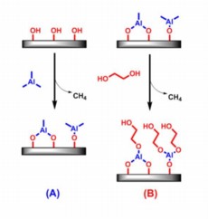
In its most common form, MLD can be used to make self-limiting, conformal, pinhole-free films of metal-organic materials called metalcones. The first example of this sort was the synthesis of "alucones" (aluminum-containing metalcones) from trimethylaluminum and ethylene glycol, as illustrated in the accompanying image above. Based upon this methodology, there is a great deal of flexibility for altering the metal as well as the organic ligand in order to fabricate hybrid thin films with customized properties. By mixing the precursors for oxide growth using ALD with those used for MLD, one can also tune the degree of incorporation of the organic component in the films.
Using this method, researchers have already tuned the elastic modulus of thin films for mechanical applications, the refractive index for optical applications, and the electrical conductivity for electronic applications. All of this means that one can tailor the properties of a surface coating "made to order". The films can then be used as is, or the organic component can alternatively be burnt off to create a material with tailored porosity for applications such as catalysis. With such a degree of tunability, the possibilities are virtually endless, as Molecular Layer Deposition helps to change the face of nanomaterials, one layer at a time.
####
For more information, please click here
Copyright © Wiley-VCH Materials Science Journals
If you have a comment, please Contact us.Issuers of news releases, not 7th Wave, Inc. or Nanotechnology Now, are solely responsible for the accuracy of the content.
Bookmark:


| Related News Press |
News and information
![]() Quantum computer improves AI predictions April 17th, 2026
Quantum computer improves AI predictions April 17th, 2026
![]() Flexible sensor gains sensitivity under pressure April 17th, 2026
Flexible sensor gains sensitivity under pressure April 17th, 2026
![]() A reusable chip for particulate matter sensing April 17th, 2026
A reusable chip for particulate matter sensing April 17th, 2026
![]() Detecting vibrational quantum beating in the predissociation dynamics of SF6 using time-resolved photoelectron spectroscopy April 17th, 2026
Detecting vibrational quantum beating in the predissociation dynamics of SF6 using time-resolved photoelectron spectroscopy April 17th, 2026
Chemistry
![]() Projecting light to dispense liquids: A new route to ultra-precise microdroplets January 30th, 2026
Projecting light to dispense liquids: A new route to ultra-precise microdroplets January 30th, 2026
![]() From sensors to smart systems: the rise of AI-driven photonic noses January 30th, 2026
From sensors to smart systems: the rise of AI-driven photonic noses January 30th, 2026
![]() "Nanoreactor" cage uses visible light for catalytic and ultra-selective cross-cycloadditions October 3rd, 2025
"Nanoreactor" cage uses visible light for catalytic and ultra-selective cross-cycloadditions October 3rd, 2025
![]() Cambridge chemists discover simple way to build bigger molecules � one carbon at a time June 6th, 2025
Cambridge chemists discover simple way to build bigger molecules � one carbon at a time June 6th, 2025
Thin films
![]() Tiny nanosheets, big leap: A new sensor detects ethanol at ultra-low levels January 30th, 2026
Tiny nanosheets, big leap: A new sensor detects ethanol at ultra-low levels January 30th, 2026
Discoveries
![]() Quantum computer improves AI predictions April 17th, 2026
Quantum computer improves AI predictions April 17th, 2026
![]() Flexible sensor gains sensitivity under pressure April 17th, 2026
Flexible sensor gains sensitivity under pressure April 17th, 2026
![]() A reusable chip for particulate matter sensing April 17th, 2026
A reusable chip for particulate matter sensing April 17th, 2026
![]() Detecting vibrational quantum beating in the predissociation dynamics of SF6 using time-resolved photoelectron spectroscopy April 17th, 2026
Detecting vibrational quantum beating in the predissociation dynamics of SF6 using time-resolved photoelectron spectroscopy April 17th, 2026
Materials/Metamaterials/Magnetoresistance
![]() First real-time observation of two-dimensional melting process: Researchers at Mainz University unveil new insights into magnetic vortex structures August 8th, 2025
First real-time observation of two-dimensional melting process: Researchers at Mainz University unveil new insights into magnetic vortex structures August 8th, 2025
![]() Researchers unveil a groundbreaking clay-based solution to capture carbon dioxide and combat climate change June 6th, 2025
Researchers unveil a groundbreaking clay-based solution to capture carbon dioxide and combat climate change June 6th, 2025
![]() A 1960s idea inspires NBI researchers to study hitherto inaccessible quantum states June 6th, 2025
A 1960s idea inspires NBI researchers to study hitherto inaccessible quantum states June 6th, 2025
![]() Institute for Nanoscience hosts annual proposal planning meeting May 16th, 2025
Institute for Nanoscience hosts annual proposal planning meeting May 16th, 2025
Announcements
![]() A fundamentally new therapeutic approach to cystic fibrosis: Nanobody repairs cellular defect April 17th, 2026
A fundamentally new therapeutic approach to cystic fibrosis: Nanobody repairs cellular defect April 17th, 2026
![]() UC Irvine physicists discover method to reverse �quantum scrambling� : The work addresses the problem of information loss in quantum computing system April 17th, 2026
UC Irvine physicists discover method to reverse �quantum scrambling� : The work addresses the problem of information loss in quantum computing system April 17th, 2026
|
|
||
|
|
||
| The latest news from around the world, FREE | ||
|
|
||
|
|
||
| Premium Products | ||
|
|
||
|
Only the news you want to read!
Learn More |
||
|
|
||
|
Full-service, expert consulting
Learn More |
||
|
|
||