Home > Press > Needle beam could eliminate signal loss in on-chip optics: Harvard researchers create a light wave that propagates without spreading
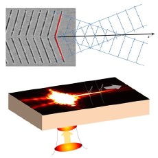 |
| Top: A micrograph and diagram of the metallic gratings that produce the needle beam. Bottom: An approximation of the experimental setup. A laser is focused from the glass substrate side onto the device. Once the non-diffractive surface wave is created, detailed information on its intensity distribution is gathered using an ultrahigh-spatial-resolution near-field scanning optical microscope. (Images courtesy of Patrice Genevet.) |
Abstract:
An international, Harvard-led team of researchers have demonstrated a new type of light beam that propagates without spreading outwards, remaining very narrow and controlled along an unprecedented distance. This "needle beam," as the team calls it, could greatly reduce signal loss for on-chip optical systems and may eventually assist the development of a more powerful class of microprocessors.
Needle beam could eliminate signal loss in on-chip optics: Harvard researchers create a light wave that propagates without spreading
Cambridge, MA | Posted on September 7th, 2012Based at the Harvard School of Engineering and Applied Sciences (SEAS) and the Laboratoire Interdisciplinaire Carnot de Bourgogne, CNRS, in France, the applied physicists both characterized and created this needle beam, which travels efficiently at the interface of gold and air. Their findings were published online August 31 in the journal Physical Review Letters.
The needle beam arises from a special class of quasiparticles called surface plasmons, which travel in tight confinement with a metal surface. The metallic stripes that carry these surface plasmons have the potential to replace standard copper electrical interconnects in microprocessors, enabling ultrafast on-chip communications.
One of the fundamental problems that has so far hindered the development of such optical interconnects is the fact that all waves naturally spread laterally during propagation, a phenomenon known as diffraction. This reduces the portion of the signal that can actually be detected.
"We have made a major step toward solving this problem by discovering and experimentally confirming the existence of a previously overlooked solution of Maxwell's equations that govern all light phenomena," says principal investigator Federico Capasso, Robert L. Wallace Professor of Applied Physics and Vinton Hayes Senior Research Fellow in Electrical Engineering at SEAS. "The solution is a highly localized surface plasmon wave that propagates for a long distance, approximately 80 microns in our experiments, in a straight line without any diffraction."
The so-called needle beam, the technical term for which is a cosine-Gauss plasmon beam, propagates in tight confinement with a nanostructured metal surface. Lead author Jiao Lin, a visiting postdoctoral fellow at SEAS from the Singapore Institute of Manufacturing and Technology, and coauthor Patrice Genevet, a research associate in Capasso's group, found an ingenious way to demonstrate the theorized phenomenon. They sculpted two sets of grooves into a gold film that was plated onto the surface of a glass sheet. These tiny grooves intersect at an angle to form a metallic grating. When illuminated by a laser, the device launches two tilted, plane surface waves which interfere constructively to create the non-diffracting beam.
"Our French colleagues did a beautiful experiment, using an ultrahigh-resolution microscope to image the needle-shaped beam propagating for a long distance across the gold surface," says Genevet.
Capasso's team hopes the finding will assist the development of more energy-efficient and powerful microprocessors.
Coauthors at CNRS included Jean Dellinger, Benoit Cluzel, and group leader Frederique de Fornel.
This work was partially supported by the U.S. Air Force Office of Scientific Research. The researchers also benefited individually from the support of the Agency for Science, Technology, and Research, Singapore, and the Robert A. Welch Foundation. Devices were fabricated at Harvard's Center for Nanoscale Systems, a member of the National Nanotechnology Infrastructure Network, funded by the National Science Foundation.
Additional images, including a comparison of the simulated result and the experimental result, are available to the media upon request.
####
For more information, please click here
Contacts:
Caroline Perry
617-496-1351
Copyright © Harvard's School of Engineering and Applied Sciences (SEAS)
If you have a comment, please Contact us.Issuers of news releases, not 7th Wave, Inc. or Nanotechnology Now, are solely responsible for the accuracy of the content.
Bookmark:


| Related News Press |
News and information
![]() Quantum computer improves AI predictions April 17th, 2026
Quantum computer improves AI predictions April 17th, 2026
![]() Flexible sensor gains sensitivity under pressure April 17th, 2026
Flexible sensor gains sensitivity under pressure April 17th, 2026
![]() A reusable chip for particulate matter sensing April 17th, 2026
A reusable chip for particulate matter sensing April 17th, 2026
![]() Detecting vibrational quantum beating in the predissociation dynamics of SF6 using time-resolved photoelectron spectroscopy April 17th, 2026
Detecting vibrational quantum beating in the predissociation dynamics of SF6 using time-resolved photoelectron spectroscopy April 17th, 2026
Govt.-Legislation/Regulation/Funding/Policy
![]() Quantum computer improves AI predictions April 17th, 2026
Quantum computer improves AI predictions April 17th, 2026
![]() Metasurfaces smooth light to boost magnetic sensing precision January 30th, 2026
Metasurfaces smooth light to boost magnetic sensing precision January 30th, 2026
![]() New imaging approach transforms study of bacterial biofilms August 8th, 2025
New imaging approach transforms study of bacterial biofilms August 8th, 2025
Chip Technology
![]() A reusable chip for particulate matter sensing April 17th, 2026
A reusable chip for particulate matter sensing April 17th, 2026
![]() Metasurfaces smooth light to boost magnetic sensing precision January 30th, 2026
Metasurfaces smooth light to boost magnetic sensing precision January 30th, 2026
Optical computing/Photonic computing
![]() ICFO researchers overcome long-standing bottleneck in single photon detection with twisted 2D materials August 8th, 2025
ICFO researchers overcome long-standing bottleneck in single photon detection with twisted 2D materials August 8th, 2025
![]() Programmable electron-induced color router array May 14th, 2025
Programmable electron-induced color router array May 14th, 2025
Discoveries
![]() Quantum computer improves AI predictions April 17th, 2026
Quantum computer improves AI predictions April 17th, 2026
![]() Flexible sensor gains sensitivity under pressure April 17th, 2026
Flexible sensor gains sensitivity under pressure April 17th, 2026
![]() A reusable chip for particulate matter sensing April 17th, 2026
A reusable chip for particulate matter sensing April 17th, 2026
![]() Detecting vibrational quantum beating in the predissociation dynamics of SF6 using time-resolved photoelectron spectroscopy April 17th, 2026
Detecting vibrational quantum beating in the predissociation dynamics of SF6 using time-resolved photoelectron spectroscopy April 17th, 2026
Announcements
![]() A fundamentally new therapeutic approach to cystic fibrosis: Nanobody repairs cellular defect April 17th, 2026
A fundamentally new therapeutic approach to cystic fibrosis: Nanobody repairs cellular defect April 17th, 2026
![]() UC Irvine physicists discover method to reverse �quantum scrambling� : The work addresses the problem of information loss in quantum computing system April 17th, 2026
UC Irvine physicists discover method to reverse �quantum scrambling� : The work addresses the problem of information loss in quantum computing system April 17th, 2026
Military
![]() Quantum engineers �squeeze� laser frequency combs to make more sensitive gas sensors January 17th, 2025
Quantum engineers �squeeze� laser frequency combs to make more sensitive gas sensors January 17th, 2025
![]() Chainmail-like material could be the future of armor: First 2D mechanically interlocked polymer exhibits exceptional flexibility and strength January 17th, 2025
Chainmail-like material could be the future of armor: First 2D mechanically interlocked polymer exhibits exceptional flexibility and strength January 17th, 2025
![]() Single atoms show their true color July 5th, 2024
Single atoms show their true color July 5th, 2024
![]() NRL charters Navy�s quantum inertial navigation path to reduce drift April 5th, 2024
NRL charters Navy�s quantum inertial navigation path to reduce drift April 5th, 2024
Photonics/Optics/Lasers
![]() Metasurfaces smooth light to boost magnetic sensing precision January 30th, 2026
Metasurfaces smooth light to boost magnetic sensing precision January 30th, 2026
![]() From sensors to smart systems: the rise of AI-driven photonic noses January 30th, 2026
From sensors to smart systems: the rise of AI-driven photonic noses January 30th, 2026
Research partnerships
![]() Lab to industry: InSe wafer-scale breakthrough for future electronics August 8th, 2025
Lab to industry: InSe wafer-scale breakthrough for future electronics August 8th, 2025
![]() HKU physicists uncover hidden order in the quantum world through deconfined quantum critical points April 25th, 2025
HKU physicists uncover hidden order in the quantum world through deconfined quantum critical points April 25th, 2025
|
|
||
|
|
||
| The latest news from around the world, FREE | ||
|
|
||
|
|
||
| Premium Products | ||
|
|
||
|
Only the news you want to read!
Learn More |
||
|
|
||
|
Full-service, expert consulting
Learn More |
||
|
|
||