Home > Press > New technique could mean super thin, strong graphene-based circuits
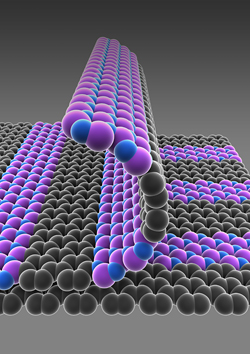 |
| Provided/Jiwoong Park Schematic illustration of single-atom-thick films with patterned regions of conducting graphene (gray) and insulating boron nitride (purple-blue). |
Abstract:
Integrated circuits, which are in everything from coffeemakers to computers and are patterned from perfectly crystalline silicon, are quite thin -- but Cornell researchers think they can push thin-film boundaries to the single-atom level.
New technique could mean super thin, strong graphene-based circuits
Ithaca, NY | Posted on August 29th, 2012Their materials of choice are graphene, single atom-thick sheets of repeating carbon atoms, and hexagonal boron nitride, similarly thin sheets of repeating boron and nitrogen atoms. Researchers led by Jiwoong Park, assistant professor of chemistry and chemical biology, have invented a way to pattern single atom films of graphene and boron nitride, an insulator, without the use of a silicon substrate. The work is detailed in an article in the journal Nature, published online Aug. 30.
The technique, which they call patterned regrowth, could lead to substrate-free, atomically thin circuits -- so thin, they could float on water or through air, but with tensile strength and top-notch electrical performance.
"We know how to grow graphene in single atom-thick films, and we know how to grow boron nitride," Park said. "But can we bring them together side and side? And when you bring them together, what happens at their junctions?"
As it turns out, researchers' patterned regrowth, which harnesses the same basic photolithography technology used in silicon wafer processing, allows graphene and boron nitride to grow in perfectly flat, structurally smooth films -- no creases or bumps, like a well-knitted scarf -- which, if combined with the final, yet to be realized step of introducing a semiconductor material, could lead to the first atomically thin integrated circuit.
Simple really is beautiful, especially in the case of thin films, because photolithography is a well-established technique that forms the basis for making integrated circuits by laying materials, one layer at a time, on flat silicon.
Patterned regrowth is a bit like stenciling, Park said. He and colleagues first grew graphene on copper and used photolithography to expose graphene on selected areas, depending on the desired pattern. They filled that exposed copper surface with boron nitride, the insulator, which grows on copper and "fills the gaps in very nicely."
"In the end, it forms a very nice cloth you just peel off," Park said.
The research team, which includes David A. Muller, professor of applied and engineering physics, is working to determine what material would best work with graphene-boron nitride thin films to make up the final semiconducting layer that could turn the films into actual devices.
The team was helped by already being skilled at making graphene -- still relatively new in the materials world -- as well as Muller's expertise in electron microscopy characterization at the nanoscale. Muller helped the team confirm that the lateral junctions of the two materials were, indeed, smooth and well connected.
The paper's co-first authors were chemistry graduate student Mark Levendorf and postdoctoral associate Cheol-Joo Kim, who fabricated the graphene and boron nitride samples and also performed the patterned regrowth at the Cornell NanoScale Science and Technology Facility.
The work was supported primarily by the Air Force Office of Scientific Research, and the National Science Foundation through the Cornell Center for Materials Research.
####
For more information, please click here
Contacts:
Media Contact:
Syl Kacapyr
(607) 255-7701
Cornell Chronicle:
Anne Ju
(607) 255-9735
Copyright © Cornell University
If you have a comment, please Contact us.Issuers of news releases, not 7th Wave, Inc. or Nanotechnology Now, are solely responsible for the accuracy of the content.
Bookmark:


| Related News Press |
News and information
![]() Quantum computer improves AI predictions April 17th, 2026
Quantum computer improves AI predictions April 17th, 2026
![]() Flexible sensor gains sensitivity under pressure April 17th, 2026
Flexible sensor gains sensitivity under pressure April 17th, 2026
![]() A reusable chip for particulate matter sensing April 17th, 2026
A reusable chip for particulate matter sensing April 17th, 2026
![]() Detecting vibrational quantum beating in the predissociation dynamics of SF6 using time-resolved photoelectron spectroscopy April 17th, 2026
Detecting vibrational quantum beating in the predissociation dynamics of SF6 using time-resolved photoelectron spectroscopy April 17th, 2026
Thin films
![]() Tiny nanosheets, big leap: A new sensor detects ethanol at ultra-low levels January 30th, 2026
Tiny nanosheets, big leap: A new sensor detects ethanol at ultra-low levels January 30th, 2026
Graphene/ Graphite
![]() Electrifying results shed light on graphene foam as a potential material for lab grown cartilage June 6th, 2025
Electrifying results shed light on graphene foam as a potential material for lab grown cartilage June 6th, 2025
![]() Breakthrough in proton barrier films using pore-free graphene oxide: Kumamoto University researchers achieve new milestone in advanced coating technologies September 13th, 2024
Breakthrough in proton barrier films using pore-free graphene oxide: Kumamoto University researchers achieve new milestone in advanced coating technologies September 13th, 2024
Govt.-Legislation/Regulation/Funding/Policy
![]() Quantum computer improves AI predictions April 17th, 2026
Quantum computer improves AI predictions April 17th, 2026
![]() Metasurfaces smooth light to boost magnetic sensing precision January 30th, 2026
Metasurfaces smooth light to boost magnetic sensing precision January 30th, 2026
![]() New imaging approach transforms study of bacterial biofilms August 8th, 2025
New imaging approach transforms study of bacterial biofilms August 8th, 2025
Discoveries
![]() Quantum computer improves AI predictions April 17th, 2026
Quantum computer improves AI predictions April 17th, 2026
![]() Flexible sensor gains sensitivity under pressure April 17th, 2026
Flexible sensor gains sensitivity under pressure April 17th, 2026
![]() A reusable chip for particulate matter sensing April 17th, 2026
A reusable chip for particulate matter sensing April 17th, 2026
![]() Detecting vibrational quantum beating in the predissociation dynamics of SF6 using time-resolved photoelectron spectroscopy April 17th, 2026
Detecting vibrational quantum beating in the predissociation dynamics of SF6 using time-resolved photoelectron spectroscopy April 17th, 2026
Announcements
![]() A fundamentally new therapeutic approach to cystic fibrosis: Nanobody repairs cellular defect April 17th, 2026
A fundamentally new therapeutic approach to cystic fibrosis: Nanobody repairs cellular defect April 17th, 2026
![]() UC Irvine physicists discover method to reverse �quantum scrambling� : The work addresses the problem of information loss in quantum computing system April 17th, 2026
UC Irvine physicists discover method to reverse �quantum scrambling� : The work addresses the problem of information loss in quantum computing system April 17th, 2026
Military
![]() Quantum engineers �squeeze� laser frequency combs to make more sensitive gas sensors January 17th, 2025
Quantum engineers �squeeze� laser frequency combs to make more sensitive gas sensors January 17th, 2025
![]() Chainmail-like material could be the future of armor: First 2D mechanically interlocked polymer exhibits exceptional flexibility and strength January 17th, 2025
Chainmail-like material could be the future of armor: First 2D mechanically interlocked polymer exhibits exceptional flexibility and strength January 17th, 2025
![]() Single atoms show their true color July 5th, 2024
Single atoms show their true color July 5th, 2024
![]() NRL charters Navy�s quantum inertial navigation path to reduce drift April 5th, 2024
NRL charters Navy�s quantum inertial navigation path to reduce drift April 5th, 2024
|
|
||
|
|
||
| The latest news from around the world, FREE | ||
|
|
||
|
|
||
| Premium Products | ||
|
|
||
|
Only the news you want to read!
Learn More |
||
|
|
||
|
Full-service, expert consulting
Learn More |
||
|
|
||