Home > Press > Bruker Introduces New Nanoelectrical AFM Mode: PeakForce KPFM Enables Quantitative Nanoscale Surface Potential Measurements
 |
Abstract:
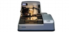
Bruker announced today the release of the new PeakForce Kelvin Probe Force Microscopy (KPFM) mode for its line of atomic force microscopes (AFMs). PeakForce KPFM™ utilizes frequency-modulation detection to provide the highest spatial resolution Kelvin probe data. It builds on Bruker's exclusive PeakForce Tapping™ technology to provide directly correlated quantitative nanomechanical data, which improves the sensitivity of the frequency-modulation measurement and eliminates artifacts. In addition, PeakForce KPFM provides a completely automated parameter setup with ScanAsyst®. The result is a significant improvement in quantitative surface potential data for materials research as well as semiconductor applications.
Bruker Introduces New Nanoelectrical AFM Mode: PeakForce KPFM Enables Quantitative Nanoscale Surface Potential Measurements
Santa Barbara, CA | Posted on August 13th, 2012 "Our research and industrial customers have increasing needs for quantitative nanoscale property measurements," said Mark R. Munch, Ph.D., President of Bruker Nano Surfaces Division. "Our new PeakForce KPFM mode combines leading-edge spatial resolution with unprecedented sensitivity and accuracy in work function measurements."
"We are committed to move AFM beyond just imaging contrast to quantitative electrical and mechanical property maps," added David V. Rossi, Executive Vice President and General Manager of Bruker's AFM Business Unit. "To enable this advance, we are building on our exclusive PeakForce Tapping technology with PeakForce QNM®, PeakForce TUNA™, and now PeakForce KPFM."
####
About Bruker Corporation
Bruker Corporation is a leading provider of high-performance scientific instruments and solutions for molecular and materials research, as well as for industrial and applied analysis. For more information about Bruker Corporation, please visit www.bruker.com.
About PeakForce KPFM
The PeakForce KPFM accessory is an optional addition available for the Dimension Icon® and MultiMode® 8 AFMs. It includes the complete set of KPFM detection mechanisms (amplitude and frequency modulation), in conjunction with both TappingMode and Peak Force Tapping, as well as the ability to perform KPFM measurements over an extended voltage range. Its signature PeakForce KPFM mode combines FM-KPFM detection with PeakForce Tapping technology. This combination enables more sensitive potential detection with optimized probes. It eliminates the contamination of FM-KPFM signals with mechanical cross-talk, retaining more accurate measurements even on samples with significant variation in adhesion or modulus. Those variations can be mapped simultaneously and independently at highest spatial resolution using PeakForce QNM. The ScanAsyst concept has been extended to KPFM, providing fully automated parameter setup to guarantee optimized results.
For more information, please click here
Contacts:
Bruker Nano Surfaces Division
Stephen Hopkins
+1 520-741-1044 x1022
Marketing Communications
Copyright © Business Wire
If you have a comment, please Contact us.Issuers of news releases, not 7th Wave, Inc. or Nanotechnology Now, are solely responsible for the accuracy of the content.
Bookmark:


| Related News Press |
News and information
![]() Quantum computer improves AI predictions April 17th, 2026
Quantum computer improves AI predictions April 17th, 2026
![]() Flexible sensor gains sensitivity under pressure April 17th, 2026
Flexible sensor gains sensitivity under pressure April 17th, 2026
![]() A reusable chip for particulate matter sensing April 17th, 2026
A reusable chip for particulate matter sensing April 17th, 2026
![]() Detecting vibrational quantum beating in the predissociation dynamics of SF6 using time-resolved photoelectron spectroscopy April 17th, 2026
Detecting vibrational quantum beating in the predissociation dynamics of SF6 using time-resolved photoelectron spectroscopy April 17th, 2026
Imaging
![]() Simple algorithm paired with standard imaging tool could predict failure in lithium metal batteries August 8th, 2025
Simple algorithm paired with standard imaging tool could predict failure in lithium metal batteries August 8th, 2025
Announcements
![]() A fundamentally new therapeutic approach to cystic fibrosis: Nanobody repairs cellular defect April 17th, 2026
A fundamentally new therapeutic approach to cystic fibrosis: Nanobody repairs cellular defect April 17th, 2026
![]() UC Irvine physicists discover method to reverse ‘quantum scrambling’ : The work addresses the problem of information loss in quantum computing system April 17th, 2026
UC Irvine physicists discover method to reverse ‘quantum scrambling’ : The work addresses the problem of information loss in quantum computing system April 17th, 2026
Tools
![]() Metasurfaces smooth light to boost magnetic sensing precision January 30th, 2026
Metasurfaces smooth light to boost magnetic sensing precision January 30th, 2026
![]() From sensors to smart systems: the rise of AI-driven photonic noses January 30th, 2026
From sensors to smart systems: the rise of AI-driven photonic noses January 30th, 2026
![]() Japan launches fully domestically produced quantum computer: Expo visitors to experience quantum computing firsthand August 8th, 2025
Japan launches fully domestically produced quantum computer: Expo visitors to experience quantum computing firsthand August 8th, 2025
|
|
||
|
|
||
| The latest news from around the world, FREE | ||
|
|
||
|
|
||
| Premium Products | ||
|
|
||
|
Only the news you want to read!
Learn More |
||
|
|
||
|
Full-service, expert consulting
Learn More |
||
|
|
||