Home > Press > Could silicene be the future of electronics?
 |
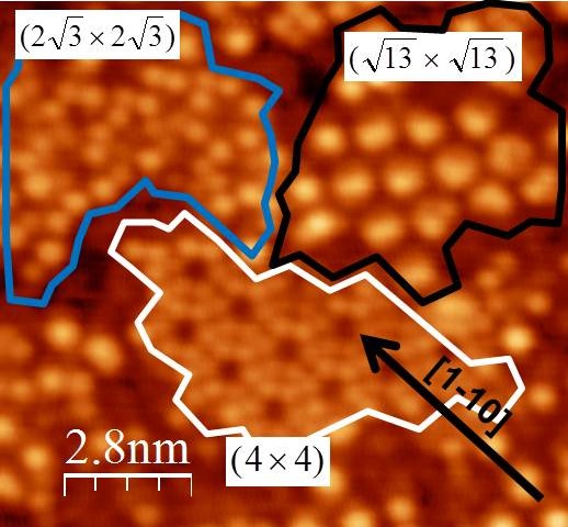
| STM image of the various surface domains of silicene |
Abstract:
The current standard in computer architecture is based upon silicon technology, which is what allows you to read this webpage, for instance, and its revolutionary influence during the digital age now leaves almost no corner of modern life untouched. In order to meet our increasing demands for more memory and for higher speed, the dimensions of the silicon-based devices which make up our computers continue to get smaller. As we begin to reach the limits of the current form of this technology, the question is what is next? According to recent work by Alessandro Molle and co-workers, the next generation of computing could be performed with silicene, an atomically thin form of silicon which has the potential to revolutionize nanoelectronics.
Could silicene be the future of electronics?
Germany | Posted on August 2nd, 2012The silicene structure consists of one atomic layer of silicon atoms and in this way it is analogous to graphene, the atomically thin sheet of carbon atoms which has been the subject of high research interest in recent years. For all of graphene's promise, one of its limitations is the lack of a naturally occurring band gap in its electronic states. This band gap is of fundamental importance for creating the electronic switches and logic circuits which make up digital electronic devices. There has been some recent progress in inducing a band gap into graphene, but it involves complicated methods such as bringing the graphene sheets into contact with a strongly-interacting substrate, which can sufficiently perturb the electronic properties. Alternatively, silicene exhibits a band gap even without modification and, it has the advantage of inherent compatibility with the silicon technology infrastructure already used in manufacturing much of today's digital electronics.
In Molle's studies, his team grew thin layers of silicene on silver substrates using molecular beam epitaxy. Using scanning tunneling microscopy, various domains of silicene were observed, showing drastically different surface symmetries as illustrated in the accompanying image above. Using tunneling spectroscopy, the researchers were able to show that the buckled structures, where the strict 2-dimensional symmetry was broken, exhibited qualitatively different electronic properties than the non-buckled phases. Understanding the details of these structure-property relationships is very important for controlling the electrical properties of the silicene thin films, and with further study, the emergence of the different silicene structures could be controlled by tailoring the growth conditions. Once these issues have been overcome, the next generation of computers may still be made of silicon after all - only thinner.
####
For more information, please click here
Copyright © Wiley-VCH Materials Science Journals
If you have a comment, please Contact us.Issuers of news releases, not 7th Wave, Inc. or Nanotechnology Now, are solely responsible for the accuracy of the content.
| Related News Press |
Thin films
![]() Tiny nanosheets, big leap: A new sensor detects ethanol at ultra-low levels January 30th, 2026
Tiny nanosheets, big leap: A new sensor detects ethanol at ultra-low levels January 30th, 2026
![]() Utilizing palladium for addressing contact issues of buried oxide thin film transistors April 5th, 2024
Utilizing palladium for addressing contact issues of buried oxide thin film transistors April 5th, 2024
![]() Understanding the mechanism of non-uniform formation of diamond film on tools: Paving the way to a dry process with less environmental impact March 24th, 2023
Understanding the mechanism of non-uniform formation of diamond film on tools: Paving the way to a dry process with less environmental impact March 24th, 2023
![]() New study introduces the best graphite films: The work by Distinguished Professor Feng Ding at UNIST has been published in the October 2022 issue of Nature Nanotechnology November 4th, 2022
New study introduces the best graphite films: The work by Distinguished Professor Feng Ding at UNIST has been published in the October 2022 issue of Nature Nanotechnology November 4th, 2022
|
|
||
|
|
||
| The latest news from around the world, FREE | ||
|
|
||
|
|
||
| Premium Products | ||
|
|
||
|
Only the news you want to read!
Learn More |
||
|
|
||
|
Full-service, expert consulting
Learn More |
||
|
|
||


