Home > Press > New technique lets scientists peer within nanoparticles, see atomic structure in 3-D
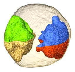 |
| Inside a gold nanoparticle |
Abstract:
UCLA researchers are now able to peer deep within the world's tiniest structures to create three-dimensional images of individual atoms and their positions. Their research, published March 22 in the journal Nature, presents a new method for directly measuring the atomic structure of nanomaterials.
New technique lets scientists peer within nanoparticles, see atomic structure in 3-D
Los Angeles, CA | Posted on March 22nd, 2012"This is the first experiment where we can directly see local structures in three dimensions at atomic-scale resolution � that's never been done before," said Jianwei (John) Miao, a professor of physics and astronomy and a researcher with the California NanoSystems Institute (CNSI) at UCLA.
Miao and his colleagues used a scanning transmission electron microscope to sweep a narrow beam of high-energy electrons over a tiny gold particle only 10 nanometers in diameter (almost 1,000 times smaller than a red blood cell). The nanoparticle contained tens of thousands of individual gold atoms, each about a million times smaller than the width of a human hair. These atoms interact with the electrons passing through the sample, casting shadows that hold information about the nanoparticle's interior structure onto a detector below the microscope.
Miao's team discovered that by taking measurements at 69 different angles, they could combine the data gleaned from each individual shadow into a 3-D reconstruction of the interior of the nanoparticle. Using this method, which is known as electron tomography, Miao's team was able to directly see individual atoms and how they were positioned inside the specific gold nanoparticle.
Presently, X-ray crystallography is the primary method for visualizing 3-D molecular structures at atomic resolutions. However, this method involves measuring many nearly identical samples and averaging the results. X-ray crystallography typically takes an average across trillions of molecules, which causes some information to get lost in the process, Miao said.
"It is like averaging together everyone on Earth to get an idea of what a human being looks like � you completely miss the unique characteristics of each individual," he said.
X-ray crystallography is a powerful technique for revealing the structure of perfect crystals, which are materials with an unbroken honeycomb of perfectly spaced atoms lined up as neatly as books on a shelf. Yet most structures existing in nature are non-crystalline, with structures far less ordered than their crystalline counterparts � picture a rock concert mosh pit rather than soldiers on parade.
"Our current technology is mainly based on crystal structures because we have ways to analyze them," Miao said. "But for non-crystalline structures, no direct experiments have seen atomic structures in three dimensions before."
Probing non-crystalline materials is important because even small variations in structure can greatly alter the electronic properties of a material, Miao noted. The ability to closely examine the inside of a semiconductor, for example, might reveal hidden internal flaws that could affect its performance.
"The three-dimensional atomic resolution of non-crystalline structures remains a major unresolved problem in the physical sciences," he said.
Miao and his colleagues haven't quite cracked the non-crystalline conundrum, but they have shown they can image a structure that isn't perfectly crystalline at a resolution of 2.4 angstroms (the average size of a gold atom is 2.8 angstroms). The gold nanoparticle they measured for their paper turned out to be composed of several different crystal grains, each forming a puzzle piece with atoms aligned in subtly different patterns. A nanostructure with hidden crystalline segments and boundaries inside will behave differently from one made of a single continuous crystal � but other techniques would have been unable to visualize them in three dimensions, Miao said.
Miao's team also found that the small golden blob they studied was in fact shaped like a multi-faceted gem, though slightly squashed on one side from resting on a flat stage inside the gigantic microscope � another small detail that might have been averaged away when using more traditional methods.
This project was inspired by Miao's earlier research, which involved finding ways to minimize the radiation dose administered to patients during CT scans. During a scan, patients must be X-rayed at a variety of angles, and those measurements are combined to give doctors a picture of what's inside the body. Miao found a mathematically more efficient way to obtain similar high-resolution images while taking scans at fewer angles. He later realized that this discovery could benefit scientists probing the insides of nanostructures, not just doctors on the lookout for tumors or fractures.
Nanostructures, like patients, can be damaged if too many scans are administered. A constant bombardment of high-energy electrons can cause the atoms in nanoparticles to be rearranged and the particle itself to change shape. By bringing his medical discovery to his work in materials science and nanoscience, Miao was able to invent a new way to peer inside the field's tiniest structures.
The discovery made by Miao's team may lead to improvements in resolution and image quality for tomography research across many fields, including the study of biological samples.
This research was conducted at CNSI's Electron Imaging Center for NanoMachines and funded by UC Discovery/Tomosoft Technologies. Tomosoft Technologies is a start-up company based on Miao's work.
Other UCLA co-authors included Chris Regan, an assistant professor of physics and astronomy and a CNSI researcher; graduate students Mary Scott, Chien-Chun Chen, Matthew Mecklenburg and Chun Zhu; and postdoctoral scholar Rui Xu. In particular, Chen and Scott played an important role in this work. Peter Ercius and Ulrich Dahmen from the National Center for Electron Microscopy at Lawrence Berkeley National Laboratory are also co-authors.
####
About University of California - Los Angeles
UCLA is California's largest university, with an enrollment of nearly 38,000 undergraduate and graduate students. The UCLA College of Letters and Science and the university's 11 professional schools feature renowned faculty and offer 337 degree programs and majors. UCLA is a national and international leader in the breadth and quality of its academic, research, health care, cultural, continuing education and athletic programs. Six alumni and five faculty have been awarded the Nobel Prize.
For more news, visit the UCLA Newsroom and follow us on Twitter.
For more information, please click here
Contacts:
Kim DeRose
Copyright © University of California - Los Angeles
If you have a comment, please Contact us.Issuers of news releases, not 7th Wave, Inc. or Nanotechnology Now, are solely responsible for the accuracy of the content.
Bookmark:


| Related News Press |
News and information
![]() Quantum computer improves AI predictions April 17th, 2026
Quantum computer improves AI predictions April 17th, 2026
![]() Flexible sensor gains sensitivity under pressure April 17th, 2026
Flexible sensor gains sensitivity under pressure April 17th, 2026
![]() A reusable chip for particulate matter sensing April 17th, 2026
A reusable chip for particulate matter sensing April 17th, 2026
![]() Detecting vibrational quantum beating in the predissociation dynamics of SF6 using time-resolved photoelectron spectroscopy April 17th, 2026
Detecting vibrational quantum beating in the predissociation dynamics of SF6 using time-resolved photoelectron spectroscopy April 17th, 2026
Imaging
![]() Simple algorithm paired with standard imaging tool could predict failure in lithium metal batteries August 8th, 2025
Simple algorithm paired with standard imaging tool could predict failure in lithium metal batteries August 8th, 2025
![]() First real-time observation of two-dimensional melting process: Researchers at Mainz University unveil new insights into magnetic vortex structures August 8th, 2025
First real-time observation of two-dimensional melting process: Researchers at Mainz University unveil new insights into magnetic vortex structures August 8th, 2025
![]() New imaging approach transforms study of bacterial biofilms August 8th, 2025
New imaging approach transforms study of bacterial biofilms August 8th, 2025
Laboratories
![]() Researchers develop molecular qubits that communicate at telecom frequencies October 3rd, 2025
Researchers develop molecular qubits that communicate at telecom frequencies October 3rd, 2025
Govt.-Legislation/Regulation/Funding/Policy
![]() Quantum computer improves AI predictions April 17th, 2026
Quantum computer improves AI predictions April 17th, 2026
![]() Metasurfaces smooth light to boost magnetic sensing precision January 30th, 2026
Metasurfaces smooth light to boost magnetic sensing precision January 30th, 2026
![]() New imaging approach transforms study of bacterial biofilms August 8th, 2025
New imaging approach transforms study of bacterial biofilms August 8th, 2025
Discoveries
![]() Quantum computer improves AI predictions April 17th, 2026
Quantum computer improves AI predictions April 17th, 2026
![]() Flexible sensor gains sensitivity under pressure April 17th, 2026
Flexible sensor gains sensitivity under pressure April 17th, 2026
![]() A reusable chip for particulate matter sensing April 17th, 2026
A reusable chip for particulate matter sensing April 17th, 2026
![]() Detecting vibrational quantum beating in the predissociation dynamics of SF6 using time-resolved photoelectron spectroscopy April 17th, 2026
Detecting vibrational quantum beating in the predissociation dynamics of SF6 using time-resolved photoelectron spectroscopy April 17th, 2026
Announcements
![]() A fundamentally new therapeutic approach to cystic fibrosis: Nanobody repairs cellular defect April 17th, 2026
A fundamentally new therapeutic approach to cystic fibrosis: Nanobody repairs cellular defect April 17th, 2026
![]() UC Irvine physicists discover method to reverse �quantum scrambling� : The work addresses the problem of information loss in quantum computing system April 17th, 2026
UC Irvine physicists discover method to reverse �quantum scrambling� : The work addresses the problem of information loss in quantum computing system April 17th, 2026
Research partnerships
![]() Lab to industry: InSe wafer-scale breakthrough for future electronics August 8th, 2025
Lab to industry: InSe wafer-scale breakthrough for future electronics August 8th, 2025
![]() HKU physicists uncover hidden order in the quantum world through deconfined quantum critical points April 25th, 2025
HKU physicists uncover hidden order in the quantum world through deconfined quantum critical points April 25th, 2025
|
|
||
|
|
||
| The latest news from around the world, FREE | ||
|
|
||
|
|
||
| Premium Products | ||
|
|
||
|
Only the news you want to read!
Learn More |
||
|
|
||
|
Full-service, expert consulting
Learn More |
||
|
|
||