Home > Press > Novel method for fabricating corrugated 3D carbon nanotube microstructures
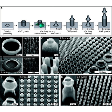 |
| Figure CNT microstructures: Fabrication of cylindrical CNT microbellows by iteration of growth and capillary forming: (A) schematic illustration of the iterative process; (B) SEM images of a cylindrical CNT microstructure before and after capillary forming (1 cycle), with close-up images emphasizing the densification of aligned CNTs; (C�E) SEM images of microstructures after consecutive growth, forming, and growth cycles, reaching 2.5 cycles in image E. |
Abstract:
Imec, in collaboration with the University of Michigan, US, presents a new 3D structuring method for making vertically-aligned corrugated nanostructures. The method is based on an iterative sequence of chemical vapor deposition (CVD) growth of carbon nanotubes (CNTs) and capillary self-assembly. A wide variety of robust 3D CNT microstructures can be fabricated, including microsprings and tilted microcantilevers. The proposed method promises the development of new microsystems, engineered surfaces and metamaterials.
Novel method for fabricating corrugated 3D carbon nanotube microstructures
Leuven, Belgium | Posted on December 16th, 2011Researchers from imec and the University of Michigan present a method that for the first time allows the stacking of sequentially folded CNT micro-architectures. Arrays of such structures with a great variety of lateral dimensions (i.e., from <10�m to >100 �m) can be fabricated in close proximity on the same substrate, thus enabling integration of heterogeneous architectures in a scalable way. The attractive properties of the CNTs suggest that the method will find several new applications. Examples are the development of new microsystems with novel functionalities, as well as engineered materials such as omniphobic surfaces and dry adhesives.
The process starts by lithographic patterning of a catalyst film on a Si wafer, followed by growth of vertically-aligned CNT microstructures by thermal CVD at atmospheric pressure. Next, the straight CNT microstructures are transformed into sloped shapes by condensation and subsequent evaporation of liquid on the surface, the so-called capillary forming step. These two process steps can then be iterated and finally result in 3D corrugated structures. Arrays of such structures with varying lateral dimensions can be fabricated as illustrated below. This study further focuses on the fabrication of (arrays of) CNT �bellows' and CNT �cantilevers'.
First, the utility of cylindrical CNT �bellows' for use as vertical microsprings was investigated. It was found that the properties of the corrugated CNT microsprings can be tuned on the basis of their geometry alone. E.g., the compliance (which is the reciprocal of the stiffness) of the springs is inversely related to their wall thickness. Microspring arrays are used commercially in probecards for the testing of electronic devices. For this particular application, the availability of a method for making arrays of compliant springs with small footprint is an important step forward.
Secondly, the method was used to create cantilevers. Iteration of growth and forming of semicircular shapes creates intricate overhanging cantilevers with multiple folds. These structures can be packed in dense arrays and oriented in any direction. We anticipate that these structures will be useful in the design of surfaces with anisotropic wetting properties and directional adhesives, where the asymmetric geometry, nanoscale texture, mechanical compliance and strong van der Waals attraction of the CNTs could be advantageous.
Finally, this process enables cost effective fabrication of vertical CNT walls with a thickness below 300 nm, and aspect ratios exceeding 1:100.
Detailed results have been published in ACS-Nano, vol. 5, n� 9, 2011, pp. 7310-7317. The paper was selected to appear on the cover of the journal [link to pubs.acs.org/action/showLargeCover?issue=361281616&]. Michael De Volder, first author of the paper, was recently also co-awarded the University of Michigan Robert M. Caddell Award along with his teammates Sameh Tawfick, Sei Jin Park, Davor Copic, and Prof. John Hart, for their work on the integration of carbon nanotubes (CNTs) in microsystems. Finally, a collection of SEM images of these corrugated CNTs structures were awarded the 1st prize at the �Science as Art Competition 2011' of the Material Research Society www.mrs.org/f11-science-as-art/.
####
About IMEC
Imec performs world-leading research in nanoelectronics. Imec leverages its scientific knowledge with the innovative power of its global partnerships in ICT, healthcare and energy. Imec delivers industry-relevant technology solutions. In a unique high-tech environment, its international top talent is committed to providing the building blocks for a better life in a sustainable society. Imec is headquartered in Leuven, Belgium, and has offices in Belgium, the Netherlands, Taiwan, US, China, India and Japan. Its staff of about 1,900 people includes more than 500 industrial residents and guest researchers. In 2010, imec's revenue (P&L) was 285 million euro. Further information on imec can be found at www.imec.be.
Imec is a registered trademark for the activities of IMEC International (a legal entity set up under Belgian law as a "stichting van openbaar nut�), imec Belgium (IMEC vzw supported by the Flemish Government), imec the Netherlands (Stichting IMEC Nederland, part of Holst Centre which is supported by the Dutch Government), imec Taiwan (IMEC Taiwan Co.) and imec China (IMEC Microelectronics (Shangai) Co. Ltd.) and imec India (Imec India Private Limited).
For more information, please click here
Contacts:
Hanne Degans
External Communications Officer
T: +32 16 28 17 69
Mobile: +32 486 065 175
Barbara Kalkis
Maestro Marketing & Public Relations
T : +1 408 996 9975
M : +1 408 529 4210
Copyright © IMEC
If you have a comment, please Contact us.Issuers of news releases, not 7th Wave, Inc. or Nanotechnology Now, are solely responsible for the accuracy of the content.
Bookmark:


| Related News Press |
News and information
![]() Quantum computer improves AI predictions April 17th, 2026
Quantum computer improves AI predictions April 17th, 2026
![]() Flexible sensor gains sensitivity under pressure April 17th, 2026
Flexible sensor gains sensitivity under pressure April 17th, 2026
![]() A reusable chip for particulate matter sensing April 17th, 2026
A reusable chip for particulate matter sensing April 17th, 2026
![]() Detecting vibrational quantum beating in the predissociation dynamics of SF6 using time-resolved photoelectron spectroscopy April 17th, 2026
Detecting vibrational quantum beating in the predissociation dynamics of SF6 using time-resolved photoelectron spectroscopy April 17th, 2026
Discoveries
![]() Quantum computer improves AI predictions April 17th, 2026
Quantum computer improves AI predictions April 17th, 2026
![]() Flexible sensor gains sensitivity under pressure April 17th, 2026
Flexible sensor gains sensitivity under pressure April 17th, 2026
![]() A reusable chip for particulate matter sensing April 17th, 2026
A reusable chip for particulate matter sensing April 17th, 2026
![]() Detecting vibrational quantum beating in the predissociation dynamics of SF6 using time-resolved photoelectron spectroscopy April 17th, 2026
Detecting vibrational quantum beating in the predissociation dynamics of SF6 using time-resolved photoelectron spectroscopy April 17th, 2026
Materials/Metamaterials/Magnetoresistance
![]() First real-time observation of two-dimensional melting process: Researchers at Mainz University unveil new insights into magnetic vortex structures August 8th, 2025
First real-time observation of two-dimensional melting process: Researchers at Mainz University unveil new insights into magnetic vortex structures August 8th, 2025
![]() Researchers unveil a groundbreaking clay-based solution to capture carbon dioxide and combat climate change June 6th, 2025
Researchers unveil a groundbreaking clay-based solution to capture carbon dioxide and combat climate change June 6th, 2025
![]() A 1960s idea inspires NBI researchers to study hitherto inaccessible quantum states June 6th, 2025
A 1960s idea inspires NBI researchers to study hitherto inaccessible quantum states June 6th, 2025
![]() Institute for Nanoscience hosts annual proposal planning meeting May 16th, 2025
Institute for Nanoscience hosts annual proposal planning meeting May 16th, 2025
Announcements
![]() A fundamentally new therapeutic approach to cystic fibrosis: Nanobody repairs cellular defect April 17th, 2026
A fundamentally new therapeutic approach to cystic fibrosis: Nanobody repairs cellular defect April 17th, 2026
![]() UC Irvine physicists discover method to reverse �quantum scrambling� : The work addresses the problem of information loss in quantum computing system April 17th, 2026
UC Irvine physicists discover method to reverse �quantum scrambling� : The work addresses the problem of information loss in quantum computing system April 17th, 2026
Research partnerships
![]() Lab to industry: InSe wafer-scale breakthrough for future electronics August 8th, 2025
Lab to industry: InSe wafer-scale breakthrough for future electronics August 8th, 2025
![]() HKU physicists uncover hidden order in the quantum world through deconfined quantum critical points April 25th, 2025
HKU physicists uncover hidden order in the quantum world through deconfined quantum critical points April 25th, 2025
|
|
||
|
|
||
| The latest news from around the world, FREE | ||
|
|
||
|
|
||
| Premium Products | ||
|
|
||
|
Only the news you want to read!
Learn More |
||
|
|
||
|
Full-service, expert consulting
Learn More |
||
|
|
||