Home > Press > JPK reports on how graphenes are being studied using AFM to better characterize their properties at the Humboldt University in Berlin
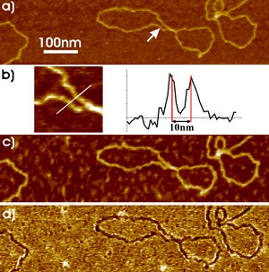 |
| Images taken on a 6 day old sample in the area of a single graphene: (a) Topography image recorded in contact mode under a normal force of 25 nN. Arrow indicates an area enlarged on (b) with two resolved DNA strands running nearly parallel to each other at a distance of 10 nm, as visualized by the inserted cross section. (c) Intermittent contact mode topography image acquired a few minutes after (a) with the same tip. (d) Intermittent contact mode phase contrast image of the same area.* |
Abstract:
JPK Instruments, a world-leading manufacturer of nanoanalytic instrumentation for research in life sciences and soft matter, reports on a keynote paper in Nano Letters where Dr Nikolai Severin and his co-workers from the group of Professor Jürgen P. Rabe have applied JPK's NanoWizard®II Ultra system to improve their understanding of the properties of graphene.
JPK reports on how graphenes are being studied using AFM to better characterize their properties at the Humboldt University in Berlin
Berlin, Germany | Posted on December 8th, 2011Physics of Macromolecules group of Professor Jürgen P. Rabe has a central research goal to correlate structure and dynamics of molecular systems at interfaces with mechanical, electronic, optical and (bio-)chemical properties from molecular to macroscopic length and time scales. Manipulation and imaging of single molecules and supramolecular systems with a scanning force microscope (SFM) is of paramount importance to the understanding of structure formation and the measurement of mechanical properties. The group is also involved in understanding and developing molecular electronics and organic electronic properties.
Within this group is Dr Nikolai Severin, recently the lead author of a paper in Nano Letters* which shows the use of AFM in the study of graphenes. The electronic properties of graphenes depend sensitively on their deformation, and therefore strain-engineered graphene electronics is envisioned. In order to deform graphenes locally, the group has mechanically exfoliated single and few layer graphenes onto atomically flat mica surfaces covered with isolated double stranded plasmid DNA rings. Using scanning force microscopy in both contact and intermittent contact modes, they have found that the graphenes replicate the topography of the underlying DNA with high precision. The availability of macromolecules of different topologies, e.g., programmable DNA patterns render this approach promising for new graphene based device designs. Furthermore, the encapsulation of single macromolecules offers new prospects for analytical scanning probe microscopy techniques.
Dr Severin has seen that graphene provides enhanced protection of DNA molecules to shear forces exerted during scanning force microscopy in contact mode. In addition, graphene will act as a surface protective layer against the ambient, e.g., against oxidation, since it is impermeable to gases. Taking into account both the high electric conductivity of graphene and its extremely small thickness, this offers new opportunities for scanning probe microscopies and spectroscopies, such as scanning tunneling or tip enhanced Raman spectroscopy for analyses of both locally deformed graphene and confined molecules. Summarising, Dr Severin said, "We have successfully demonstrated that topography of graphenes can be controlled with the precision down to single molecules, i.e. graphenes are so flexible that they can replicate the topography of single molecules, when deposited on these molecules."
He also commented on some of the reasons for choosing to work with JPK NanoWizard® II for this work: "We are able to use a relatively large size of samples and scan areas of up to 30 microns. The linearized scanner is most important for us to precisely measure the height of DNA and their cross sections. The system shows little thermal drift which is important when making measurements on such small length scales. I also found the software was quite easy to use."
For more details about JPK's specialist products and applications for the bio and nano sciences, please contact JPK on +49 30533112070, visit the web site: www.jpk.com or see more on Facebook: www.jpk.com/facebook.
* Reference acknowledgment:
Replication of Single Macromolecules with Graphene, N . Severin*†, M. Dorn†, A. Kalachev‡, and J. P. Rabe*†;†Department of Physics, Humboldt-Universitaat zu Berlin, Newtonstrasse 15, 12489 Berlin, Germany. ‡ PlasmaChem GmbH, Rudower Chaussee 29, 12489 Berlin, Germany: Nano Lett., 2011, 11 (6), pp 2436-2439; DOI: 10.1021/nl200846f; Publication Date (Web): May 16, 2011; Copyright © 2011 American Chemical Society
####
About JPK Instruments (JPK)
JPK Instruments AG is a world-leading manufacturer of nanoanalytic instruments – particularly atomic force microscope (AFM) systems and optical tweezers – for a broad range of applications reaching from soft matter physics to nano-optics, from surface chemistry to cell and molecular biology. From its earliest days applying atomic force microscope (AFM) technology, JPK has recognized the opportunities provided by nanotechnology for transforming life sciences and soft matter research. This focus has driven JPK's success in uniting the worlds of nanotechnology tools and life science applications by offering cutting-edge technology and unique applications expertise. Headquartered in Berlin and with direct operations in Dresden, Cambridge (UK), Singapore, Tokyo and Paris (France), JPK maintains a global network of distributors and support centers and provides on the spot applications and service support to an ever-growing community of researchers.
For more information, please click here
Contacts:
JPK Instruments AG
Bouchéstrasse 12
Haus 2, Aufgang C
Berlin 12435
Germany
T +49 30533112070
F +49 30 5331 22555
www.jpk.com
Talking Science Limited
39 de Bohun Court
Saffron Walden
Essex CB10 2BA
United Kingdom
T +44(0)1799 521881
M +44(0)7843 012997
www.talking-science.com
Copyright © JPK Instruments (JPK)
If you have a comment, please Contact us.Issuers of news releases, not 7th Wave, Inc. or Nanotechnology Now, are solely responsible for the accuracy of the content.
Bookmark:


| Related News Press |
News and information
![]() Quantum computer improves AI predictions April 17th, 2026
Quantum computer improves AI predictions April 17th, 2026
![]() Flexible sensor gains sensitivity under pressure April 17th, 2026
Flexible sensor gains sensitivity under pressure April 17th, 2026
![]() A reusable chip for particulate matter sensing April 17th, 2026
A reusable chip for particulate matter sensing April 17th, 2026
![]() Detecting vibrational quantum beating in the predissociation dynamics of SF6 using time-resolved photoelectron spectroscopy April 17th, 2026
Detecting vibrational quantum beating in the predissociation dynamics of SF6 using time-resolved photoelectron spectroscopy April 17th, 2026
Imaging
![]() Simple algorithm paired with standard imaging tool could predict failure in lithium metal batteries August 8th, 2025
Simple algorithm paired with standard imaging tool could predict failure in lithium metal batteries August 8th, 2025
Graphene/ Graphite
![]() Electrifying results shed light on graphene foam as a potential material for lab grown cartilage June 6th, 2025
Electrifying results shed light on graphene foam as a potential material for lab grown cartilage June 6th, 2025
![]() Breakthrough in proton barrier films using pore-free graphene oxide: Kumamoto University researchers achieve new milestone in advanced coating technologies September 13th, 2024
Breakthrough in proton barrier films using pore-free graphene oxide: Kumamoto University researchers achieve new milestone in advanced coating technologies September 13th, 2024
Announcements
![]() A fundamentally new therapeutic approach to cystic fibrosis: Nanobody repairs cellular defect April 17th, 2026
A fundamentally new therapeutic approach to cystic fibrosis: Nanobody repairs cellular defect April 17th, 2026
![]() UC Irvine physicists discover method to reverse ‘quantum scrambling’ : The work addresses the problem of information loss in quantum computing system April 17th, 2026
UC Irvine physicists discover method to reverse ‘quantum scrambling’ : The work addresses the problem of information loss in quantum computing system April 17th, 2026
Tools
![]() Metasurfaces smooth light to boost magnetic sensing precision January 30th, 2026
Metasurfaces smooth light to boost magnetic sensing precision January 30th, 2026
![]() From sensors to smart systems: the rise of AI-driven photonic noses January 30th, 2026
From sensors to smart systems: the rise of AI-driven photonic noses January 30th, 2026
![]() Japan launches fully domestically produced quantum computer: Expo visitors to experience quantum computing firsthand August 8th, 2025
Japan launches fully domestically produced quantum computer: Expo visitors to experience quantum computing firsthand August 8th, 2025
|
|
||
|
|
||
| The latest news from around the world, FREE | ||
|
|
||
|
|
||
| Premium Products | ||
|
|
||
|
Only the news you want to read!
Learn More |
||
|
|
||
|
Full-service, expert consulting
Learn More |
||
|
|
||