Home > Press > Lehigh University ceramics researchers shed light on metal embrittlement: Collaboration uses Lehigh's advanced electron microscopes to pinpoint phase transition
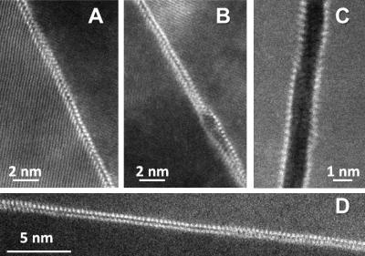 |
| STEM HAADF micrographs show 2 layers of Bi absorbed along the general GBs of a Ni polycrystal quenched from 700�C. (C) Weakly bonded Bi atoms could cause the boundaries to easily fracture between layers and thus embrittle the material. Presumably, decohesion of this GB occurred during TEM specimen preparation. (D) A bilayer interfacial phase of similar character was observed in specimens quenched from 1100�C.
Credit: Martin Harmer, Lehigh University |
Abstract:
Why does a solid metal that is engineered for ductility become brittle, often suddenly and with dramatic consequences, in the presence of certain liquid metal impurities?
Lehigh University ceramics researchers shed light on metal embrittlement: Collaboration uses Lehigh's advanced electron microscopes to pinpoint phase transition
Bethlehem, PA | Posted on September 22nd, 2011The phenomenon, known as liquid metal embrittlement, or LME, has baffled metallurgists for a century.
Now, a team of ceramics researchers has shed light on LME by obtaining atomic-scale images of unprecedented resolution of the grain boundaries, or internal interfaces, where LME occurs.
In doing so, says Martin Harmer, professor of materials science and engineering at Lehigh University, the researchers have achieved the first direct observation in a metal system of a bilayer grain boundary phase transition.
The study suggests that interior interfaces can undergo transitions similar to the solid-to-liquid and liquid-to-gas phase transitions that occur in larger, "bulk" materials.
It also paves the way for scientists to prevent LME by strengthening the chemical bonds of the materials present at grain boundaries.
"This is a very exciting discovery," says Harmer, who directs Lehigh's Center for Advanced Materials and Nanotechnology. "It gives us a much clearer understanding of the atomic mechanism of LME and it promises to improve our ability to control and fine-tune the properties of metals and other materials during fabrication."
Harmer and his colleagues reported their findings Sept. 23 in Science magazine.
Their 18-month study was funded by the U.S. Navy. The group will continue its work, with a focus on rectifying LME-related problems in metals, with help from a five-year, $7.5 million grant through the Department of Defense's Multidisciplinary University Research Initiative program. That project involves researchers from Lehigh, Carnegie-Mellon, Clemson, Illinois and Kutztown universities.
The common ground of ceramics and metals
Many of the consequences of LME affect everyday life, says Harmer.
A steel highway signpost can crack because LME weakened it by the molten zinc alloy applied to the steel during fabrication. Mercury and gallium, both liquid at room temperature, cause normally corrosion-resistant aluminum to become brittle. And concerns over LME make nuclear power plant operators hesitate to switch from water to liquid metal coolant, whose higher boiling point and ability to absorb radiation give it superior and more reliable cooling properties.
Harmer, who has spent 30 years studying ceramics, became interested in LME after he and his students in 2006 identified six grain-boundary "complexions," each with a distinct rate of grain growth, in the ceramic alumina.
He described complexions, and their influence on material properties, in an article titled "The Phase Behavior of Interfaces," http://www.sciencemag.org/content/332/6026/182.full, which was published April 8 in the Perspective section of Science.
The discovery of grain-boundary complexions in ceramics, Harmer says, prompted him to seek insight into the embrittlement of metals.
"Our ideas on complexions can be tested more rigorously with metals than with ceramics because metals are simpler systems than ceramics," he says.
Harmer's group examined a nickel-bismuth alloy using Lehigh's JEOL 2200 FS aberration-corrected scanning transmission electron microscope (STEM), which has unparalleled imaging capabilities. The group employed a technique called high-angle annular dark-field imaging (HAADF), which focuses a beam of electrons only 1 angstrom (0.1 nm) wide on a sample.
Previous studies had revealed the existence of four interfacial phases at grain boundaries (GB) in metals - a clean, or intrinsic GB, a monolayer/submonolayer, a nanometer-thick intergranular film, and a complete GB wetting film.
The aberration-corrected STEM revealed two additional GB phases - a bilayer and a trilayer.
"A bilayer had been seen before in a ceramic system," says Harmer, "but no one had seen such examples of the bi- and trilayers in metals."
The aberration-corrected STEM pinpointed the bilayer of bismuth atoms at the grain boundary as the source of a weak atomic-scale bond in the nickel-bismuth alloy.
"The bonding is so weak that the grains come apart almost like the opening of a slippery zipper," says Harmer.
"There is a very strong bond between bismuth and nickel, so it had never been clear why the alloy is prone to embrittlement. But the bonds between bismuth atoms are weak. We are the first group to see the formation of a bismuth bilayer that weakens this material."
A comprehensive study
Harmer described his group's study as "exhaustive." The researchers examined 12 independent interfaces and took care to exclude artificial "imaging artifacts" introduced by experimental error or by technology.
They also attempted to ensure that their images represented the 3-D nature of nickel-bismuth.
"When you project a 3-D image onto a 2-D film, distortions can result. To avoid this, we imaged at different depths on the sample. By looking sequentially at these images and their structural thickness, we were able to rule out artifacts that give the illusion of a bilayer."
In contrast with previous studies, most of which looked at synthetic bi-crystals, Harmer's group examined polycrystalline nickel which resembles industrial materials.
"Real grain boundaries are typically less symmetrical and have higher energy than synthetic bi-crystals," says Harmer, "and they show other differences as well."
The group plans next to attempt to experiment with the chemistry of nickel-bismuth GBs to produce a more ductile behavior.
"Perhaps combining the bismuth with other elements that bond at the interface will prove effective," says Harmer.
A new aberration-corrected microscope that Lehigh is acquiring in early 2012 - the JEOL ARM2200F STEM - will improve the group's ability to do atomic-scale chemical analysis of grain boundaries, says Harmer.
The present study, "The Role of a Bilayer Interfacial Phase on Liquid Metal Embrittlement," was written by Harmer; Jian Luo and Kaveh Meshinchi Asl of Clemson University's School of Materials Science and Engineering; Huikai Cheng, a former research scientist at Lehigh; and Christopher Kiely, director of Lehigh's Nanocharacterization Laboratory.
####
For more information, please click here
Contacts:
Jordan Reese
610-758-6656
Copyright © Lehigh University
If you have a comment, please Contact us.Issuers of news releases, not 7th Wave, Inc. or Nanotechnology Now, are solely responsible for the accuracy of the content.
Bookmark:


| Related News Press |
News and information
![]() Quantum computer improves AI predictions April 17th, 2026
Quantum computer improves AI predictions April 17th, 2026
![]() Flexible sensor gains sensitivity under pressure April 17th, 2026
Flexible sensor gains sensitivity under pressure April 17th, 2026
![]() A reusable chip for particulate matter sensing April 17th, 2026
A reusable chip for particulate matter sensing April 17th, 2026
![]() Detecting vibrational quantum beating in the predissociation dynamics of SF6 using time-resolved photoelectron spectroscopy April 17th, 2026
Detecting vibrational quantum beating in the predissociation dynamics of SF6 using time-resolved photoelectron spectroscopy April 17th, 2026
Imaging
![]() Simple algorithm paired with standard imaging tool could predict failure in lithium metal batteries August 8th, 2025
Simple algorithm paired with standard imaging tool could predict failure in lithium metal batteries August 8th, 2025
Materials/Metamaterials/Magnetoresistance
![]() First real-time observation of two-dimensional melting process: Researchers at Mainz University unveil new insights into magnetic vortex structures August 8th, 2025
First real-time observation of two-dimensional melting process: Researchers at Mainz University unveil new insights into magnetic vortex structures August 8th, 2025
![]() Researchers unveil a groundbreaking clay-based solution to capture carbon dioxide and combat climate change June 6th, 2025
Researchers unveil a groundbreaking clay-based solution to capture carbon dioxide and combat climate change June 6th, 2025
![]() A 1960s idea inspires NBI researchers to study hitherto inaccessible quantum states June 6th, 2025
A 1960s idea inspires NBI researchers to study hitherto inaccessible quantum states June 6th, 2025
![]() Institute for Nanoscience hosts annual proposal planning meeting May 16th, 2025
Institute for Nanoscience hosts annual proposal planning meeting May 16th, 2025
Announcements
![]() A fundamentally new therapeutic approach to cystic fibrosis: Nanobody repairs cellular defect April 17th, 2026
A fundamentally new therapeutic approach to cystic fibrosis: Nanobody repairs cellular defect April 17th, 2026
![]() UC Irvine physicists discover method to reverse �quantum scrambling� : The work addresses the problem of information loss in quantum computing system April 17th, 2026
UC Irvine physicists discover method to reverse �quantum scrambling� : The work addresses the problem of information loss in quantum computing system April 17th, 2026
Tools
![]() Metasurfaces smooth light to boost magnetic sensing precision January 30th, 2026
Metasurfaces smooth light to boost magnetic sensing precision January 30th, 2026
![]() From sensors to smart systems: the rise of AI-driven photonic noses January 30th, 2026
From sensors to smart systems: the rise of AI-driven photonic noses January 30th, 2026
![]() Japan launches fully domestically produced quantum computer: Expo visitors to experience quantum computing firsthand August 8th, 2025
Japan launches fully domestically produced quantum computer: Expo visitors to experience quantum computing firsthand August 8th, 2025
|
|
||
|
|
||
| The latest news from around the world, FREE | ||
|
|
||
|
|
||
| Premium Products | ||
|
|
||
|
Only the news you want to read!
Learn More |
||
|
|
||
|
Full-service, expert consulting
Learn More |
||
|
|
||