Home > Press > Electrons and Lattice Vibrations—A Strong Team in the Nano World
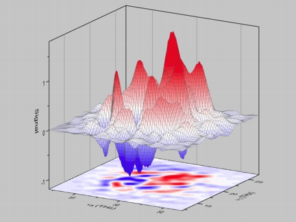 |
| Measured two-dimensional spectrum. Without the interaction of the electron with lattice vibrations there would be no signal in the range shown. |
Abstract:
Using a newly developed type of spectroscopy, Berlin researchers have shown that electrons in a semiconductor are best described as a cloud with a size of a few nanometer (one nanometer is one billionth of one meter). The cloud size is determined by the interaction of the electron with vibrations in the crystal lattice.
Electrons and Lattice Vibrations—A Strong Team in the Nano World
Berlin, Germany | Posted on August 6th, 2011Semiconductor electronics generates, controls, and amplifies electrical current in devices like the transistor. The carriers of the electric current are mobile electrons, which move with high velocities through the crystal lattice of the semiconductor. Doing this, they lose part of their kinetic energy by causing atoms in the lattice to vibrate. In semiconductors like gallium arsenide the positively and negatively charged ions of the crystal lattice vibrate with an extremely short period of 100 fs (1 fs = 10-15 s = 1 billionth part of one millionth of a second). In the microcosm of electrons and ions such vibrations are quantized. This means that the vibrational energy can only be an integer multiple of a vibrational quantum, also known as a phonon. When an electron interacts with the crystal lattice (the so called electron-phonon interaction), energy is transferred from the electron to the lattice in the form of such vibrational quanta.
Berlin researchers report in the latest issue of the scientific journal Physical Review Letters that the strength of the electron-phonon interaction depends sensitively on the electron size, i.e., on the spatial extent of its charge cloud. Experiments in the time range of the lattice vibration show that reducing the electron size leads to an increase of the interaction by up to a factor of 50. This results in a strong coupling of the movements of electrons and ions. Electron and phonon together form a new quasi particle, a polaron.
To visualize this phenomenon, the researchers used a nanostructure made from gallium arsenide and gallium aluminum arsenide, in which the energies of the movements of electrons and ions were tuned to each other. The coupling of both movements was shown by a new optical technique. Several ultrashort light pulses in the infrared excite the system under study. The subsequent emission of light by the moving charge carriers is measured in real time. In this way two-dimensional nonlinear spectra (see Fig.) are generated, which allow the detailed investigation of coupled transitions and the determination of the electron-phonon coupling strength. From the coupling strength one finds the size of the electron cloud, which is just 3-4 nanometers (1 nanometer = 10-9 m = 1 billionth of one meter). Furthermore, this new method shows for the first time the importance of electron-phonon coupling for optical spectra of semiconductors. This is of interest for the development of optoelectronic devices with custom-tailored optical and electric properties
Full bibliographic informationW. Kuehn et al., Phys. Rev. Lett. 107, 067401 (2011); J. Phys. Chem. B 115, 5448 (2011).
####
For more information, please click here
Contacts:
Christine Vollgraf
+49-30-63923337
Klaus Reimann
Michael Woerner
Thomas Elsaesser
Max-Born-Institut fuer Nichtlineare Optik und Kurzzeitspektroskopie
Tel.: +49 30 6392 1470
Copyright © AlphaGalileo
If you have a comment, please Contact us.Issuers of news releases, not 7th Wave, Inc. or Nanotechnology Now, are solely responsible for the accuracy of the content.
Bookmark:


| Related News Press |
News and information
![]() Quantum computer improves AI predictions April 17th, 2026
Quantum computer improves AI predictions April 17th, 2026
![]() Flexible sensor gains sensitivity under pressure April 17th, 2026
Flexible sensor gains sensitivity under pressure April 17th, 2026
![]() A reusable chip for particulate matter sensing April 17th, 2026
A reusable chip for particulate matter sensing April 17th, 2026
![]() Detecting vibrational quantum beating in the predissociation dynamics of SF6 using time-resolved photoelectron spectroscopy April 17th, 2026
Detecting vibrational quantum beating in the predissociation dynamics of SF6 using time-resolved photoelectron spectroscopy April 17th, 2026
Chip Technology
![]() A reusable chip for particulate matter sensing April 17th, 2026
A reusable chip for particulate matter sensing April 17th, 2026
![]() Metasurfaces smooth light to boost magnetic sensing precision January 30th, 2026
Metasurfaces smooth light to boost magnetic sensing precision January 30th, 2026
Discoveries
![]() Quantum computer improves AI predictions April 17th, 2026
Quantum computer improves AI predictions April 17th, 2026
![]() Flexible sensor gains sensitivity under pressure April 17th, 2026
Flexible sensor gains sensitivity under pressure April 17th, 2026
![]() A reusable chip for particulate matter sensing April 17th, 2026
A reusable chip for particulate matter sensing April 17th, 2026
![]() Detecting vibrational quantum beating in the predissociation dynamics of SF6 using time-resolved photoelectron spectroscopy April 17th, 2026
Detecting vibrational quantum beating in the predissociation dynamics of SF6 using time-resolved photoelectron spectroscopy April 17th, 2026
Announcements
![]() A fundamentally new therapeutic approach to cystic fibrosis: Nanobody repairs cellular defect April 17th, 2026
A fundamentally new therapeutic approach to cystic fibrosis: Nanobody repairs cellular defect April 17th, 2026
![]() UC Irvine physicists discover method to reverse ‘quantum scrambling’ : The work addresses the problem of information loss in quantum computing system April 17th, 2026
UC Irvine physicists discover method to reverse ‘quantum scrambling’ : The work addresses the problem of information loss in quantum computing system April 17th, 2026
Photonics/Optics/Lasers
![]() Metasurfaces smooth light to boost magnetic sensing precision January 30th, 2026
Metasurfaces smooth light to boost magnetic sensing precision January 30th, 2026
![]() From sensors to smart systems: the rise of AI-driven photonic noses January 30th, 2026
From sensors to smart systems: the rise of AI-driven photonic noses January 30th, 2026
|
|
||
|
|
||
| The latest news from around the world, FREE | ||
|
|
||
|
|
||
| Premium Products | ||
|
|
||
|
Only the news you want to read!
Learn More |
||
|
|
||
|
Full-service, expert consulting
Learn More |
||
|
|
||