Home > Press > New JEOL Large Angle Energy Dispersive Spectrometer (EDS) for Ultrafast Elemental Mapping of S/TEM Samples
 |
Abstract:
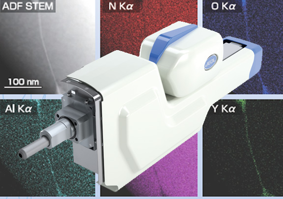
JEOL has developed a new generation of Energy Dispersive Spectrometer (EDS) for ultrafast, ultrasensitive collection of X-rays through analysis with its Scanning Transmission Electron Microscopes (S/TEM). Centurio from JEOL is a novel Silicon Drift Detector (SDD) EDS that collects X-rays from samples at an unprecedented large solid angle of up to 0.98 steradians from a detection area of 100mm2. The larger the solid angle of measurement, the more data the EDS collects to construct detailed analytical maps of the elements in the sample.
New JEOL Large Angle Energy Dispersive Spectrometer (EDS) for Ultrafast Elemental Mapping of S/TEM Samples
Peabody, MA | Posted on July 7th, 2011With the ability to efficiently collect x-rays at very high count rates, Centurio speeds elemental mapping and improves element detection sensitivity without loss of energy resolution. Large pixel number EDS maps can be made at rates ten times faster than with previous EDS designs, with excellent signal-to-noise ratio. Combined with the large probe currents in small probe sizes attainable with aberration-corrected STEM, fast, efficient atomic resolution EDS analysis is possible.
The automatically retractable side entry design allows fast repositioning to avoid irradiation from back-scattered electrons.
Centurio exponentially expands the elemental mapping capability for the JEOL 200kV and higher TEMs, including the JEM-ARM200F atomic resolution TEM with optional cold Field Emission Gun, and the new JEM-2800 automated, high throughput, nano-area analysis TEM.
www.jeolusa.com/PRODUCTS/ElectronOptics/TransmissionElectronMicroscopesTEM/Analytical/Centuriooption/tabid/811/Default.aspx
####
About JEOL USA, Inc.
JEOL is a world leader in electron optical equipment and instrumentation for high-end scientific and industrial research and development. Core product groups include electron microscopes (SEMs and TEMs), instruments for the semiconductor industry (electron beam lithography and a series of defect review and inspection tools), and analytical instruments including mass spectrometers, NMRs and ESRs.
JEOL USA, Inc., a wholly owned subsidiary of JEOL, Ltd., Japan, was incorporated in the United States in 1962. The company has 13 regional service centers that offer unlimited emergency service and support in the U.S.
For more information, please click here
Contacts:
JEOL USA, Inc.
11 Dearborn Road
Peabody, MA 01960
978-535-5900
Patricia Corkum
978-536-2273
Copyright © JEOL USA, Inc.
If you have a comment, please Contact us.Issuers of news releases, not 7th Wave, Inc. or Nanotechnology Now, are solely responsible for the accuracy of the content.
Bookmark:


| Related News Press |
News and information
![]() Quantum computer improves AI predictions April 17th, 2026
Quantum computer improves AI predictions April 17th, 2026
![]() Flexible sensor gains sensitivity under pressure April 17th, 2026
Flexible sensor gains sensitivity under pressure April 17th, 2026
![]() A reusable chip for particulate matter sensing April 17th, 2026
A reusable chip for particulate matter sensing April 17th, 2026
![]() Detecting vibrational quantum beating in the predissociation dynamics of SF6 using time-resolved photoelectron spectroscopy April 17th, 2026
Detecting vibrational quantum beating in the predissociation dynamics of SF6 using time-resolved photoelectron spectroscopy April 17th, 2026
Imaging
![]() Simple algorithm paired with standard imaging tool could predict failure in lithium metal batteries August 8th, 2025
Simple algorithm paired with standard imaging tool could predict failure in lithium metal batteries August 8th, 2025
Announcements
![]() A fundamentally new therapeutic approach to cystic fibrosis: Nanobody repairs cellular defect April 17th, 2026
A fundamentally new therapeutic approach to cystic fibrosis: Nanobody repairs cellular defect April 17th, 2026
![]() UC Irvine physicists discover method to reverse �quantum scrambling� : The work addresses the problem of information loss in quantum computing system April 17th, 2026
UC Irvine physicists discover method to reverse �quantum scrambling� : The work addresses the problem of information loss in quantum computing system April 17th, 2026
Tools
![]() Metasurfaces smooth light to boost magnetic sensing precision January 30th, 2026
Metasurfaces smooth light to boost magnetic sensing precision January 30th, 2026
![]() From sensors to smart systems: the rise of AI-driven photonic noses January 30th, 2026
From sensors to smart systems: the rise of AI-driven photonic noses January 30th, 2026
![]() Japan launches fully domestically produced quantum computer: Expo visitors to experience quantum computing firsthand August 8th, 2025
Japan launches fully domestically produced quantum computer: Expo visitors to experience quantum computing firsthand August 8th, 2025
|
|
||
|
|
||
| The latest news from around the world, FREE | ||
|
|
||
|
|
||
| Premium Products | ||
|
|
||
|
Only the news you want to read!
Learn More |
||
|
|
||
|
Full-service, expert consulting
Learn More |
||
|
|
||