Home > Press > Cameca launches new field emission electron probe microanalyzer (FE-EPMA):SXFiveFE for Quantitative Microanalysis and X-Ray Imaging at High-Spatial Resolution
 |
Abstract:
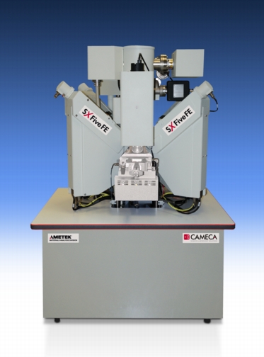
CAMECA--a world leader in scientific instrumentation and metrology solutions--has unveiled the SXFiveFE, a field emission electron probe microanalyzer (FE-EPMA) that is the latest addition to the CAMECA line of high-end microanalytical instruments.
Cameca launches new field emission electron probe microanalyzer (FE-EPMA):SXFiveFE for Quantitative Microanalysis and X-Ray Imaging at High-Spatial Resolution
Gennevilliers, France | Posted on May 23rd, 2011"We are very proud to introduce the SXFiveFE microanalyzer, because we believe it represents a major advancement in microanalysis technology," comments Georges Antier, CAMECA Vice President and Business Unit Manager. "Developed for a wide range of micro and nanoanalytical applications, the SXFiveFE EPMA is CAMECA's fifth generation electron probe microanalyzer and the culmination of our more than 50 years experience in EPMA technology.
"This highly sophisticated instrument combines proven technology from our SIMS and other EPMA products with the latest developments in general purpose EPMA, including the addition of a field emission source," he adds.
"The SXFiveFE brings together all of the best features of CAMECA's earlier electron probe microanalyzers and incorporates a number of other features, including the unique combination of a field emission electron column and CAMECA's industry-leading high-sensitivity and resolution spectrometers, that we consider a major breakthrough in microanalysis," notes Mr. Antier.
"These features along with reliability improvements from our automated EPMA for the semiconductor industry, a novel field emission source and a redesigned electron column result in a highly versatile microanalyzer with unique capabilities for quantitative microanalysis and X-Ray imaging at the highest possible spatial resolution," he concludes.
The instrument is suitable for a diverse range of applications from geochronology, mineralogy and nuclear forensics to materials, thin films and semiconductor research.
Since introducing its first commercial EPMA to the market in 1958, CAMECA has brought continuous improvements to the technology. Hundreds of CAMECA EPMA instruments are installed at major corporations as well as in renowned universities and public research institutes across the world.
The newly delivered EPMA platform is available in two configurations: SXFive with W and LaB6 sources and SXFiveFE with FE source. CAMECA has optimized the performance of both instruments for challenging microanalytical applications at sub-micron spatial resolution, extending EPMA capabilities to smaller analyzed volumes. Equipped with high-precision spectrometers for greatest reproducibility, the instrument delivers highest quality minor and trace element analysis. In addition, it offers full automation for long-term unattended analysis.
####
About CAMECA
CAMECA has more than 50 years of experience in the design, manufacture and servicing of scientific instruments for material micro- and nanoanalysis. Since pioneering Electron Probe Microanalysis (EPMA) instrumentation in the 1950s, and Secondary Ion Mass Spectrometry (SIMS) in the 1960s, CAMECA has remained an undisputed world leader, while achieving numerous breakthrough innovations in such complementary techniques as Low-energy Electron induced X-ray Emissions Spectrometry (LEXES) and Atom Probe Tomography.
More recently CAMECA has evolved successfully from a provider of scientific instrumentation for the international research community to a provider of metrology solutions for the semiconductor industry. Headquartered near Paris, CAMECA has offices in China, Germany, India, Japan, Korea, Taiwan and the United States along with a global network of agents. Acquired in 2007 by AMETEK, Inc, a leading global manufacturer of electronic instrument and electromechanical products, CAMECA is now a unit of AMETEK�s Materials Analysis Division.
For more information, please click here
Contacts:
Marion Chopin +33 (1) 43 34 62 00
CAMECA Business Unit
AMETEK Materials Analysis Division
Copyright © CAMECA
If you have a comment, please Contact us.Issuers of news releases, not 7th Wave, Inc. or Nanotechnology Now, are solely responsible for the accuracy of the content.
| Related News Press |
News and information
![]() Quantum computer improves AI predictions April 17th, 2026
Quantum computer improves AI predictions April 17th, 2026
![]() Flexible sensor gains sensitivity under pressure April 17th, 2026
Flexible sensor gains sensitivity under pressure April 17th, 2026
![]() A reusable chip for particulate matter sensing April 17th, 2026
A reusable chip for particulate matter sensing April 17th, 2026
![]() Detecting vibrational quantum beating in the predissociation dynamics of SF6 using time-resolved photoelectron spectroscopy April 17th, 2026
Detecting vibrational quantum beating in the predissociation dynamics of SF6 using time-resolved photoelectron spectroscopy April 17th, 2026
Imaging
![]() Simple algorithm paired with standard imaging tool could predict failure in lithium metal batteries August 8th, 2025
Simple algorithm paired with standard imaging tool could predict failure in lithium metal batteries August 8th, 2025
Announcements
![]() A fundamentally new therapeutic approach to cystic fibrosis: Nanobody repairs cellular defect April 17th, 2026
A fundamentally new therapeutic approach to cystic fibrosis: Nanobody repairs cellular defect April 17th, 2026
![]() UC Irvine physicists discover method to reverse �quantum scrambling� : The work addresses the problem of information loss in quantum computing system April 17th, 2026
UC Irvine physicists discover method to reverse �quantum scrambling� : The work addresses the problem of information loss in quantum computing system April 17th, 2026
Tools
![]() Metasurfaces smooth light to boost magnetic sensing precision January 30th, 2026
Metasurfaces smooth light to boost magnetic sensing precision January 30th, 2026
![]() From sensors to smart systems: the rise of AI-driven photonic noses January 30th, 2026
From sensors to smart systems: the rise of AI-driven photonic noses January 30th, 2026
![]() Japan launches fully domestically produced quantum computer: Expo visitors to experience quantum computing firsthand August 8th, 2025
Japan launches fully domestically produced quantum computer: Expo visitors to experience quantum computing firsthand August 8th, 2025
|
|
||
|
|
||
| The latest news from around the world, FREE | ||
|
|
||
|
|
||
| Premium Products | ||
|
|
||
|
Only the news you want to read!
Learn More |
||
|
|
||
|
Full-service, expert consulting
Learn More |
||
|
|
||


