Home > Press > Looking inside nanomaterials in three dimensions
 |
Abstract:
On May 13th 2011, the journal Science publishes a paper where scientists from Risř DTU in collaboration with scientists from China and USA, report a new method for revealing a 3D picture of the structure inside a material.
Looking inside nanomaterials in three dimensions
Denmark | Posted on May 19th, 2011Most solid materials are composed of millions of small crystals, packed together to form a fully dense solid. The orientations, shapes, sizes and relative arrangement of these crystals are important in determining many material properties.
Traditionally, it has only been possible to see the crystal structure of a material by looking at a cut surface, giving just 2D information. In recent years, x-ray methods have been developed that can be used to look inside a material and obtain a 3D map of the crystal structure. However, these methods have a resolution limit of around 100nm (one nanometer is 100,000 times smaller than the width of a human hair).
In contrast, the newly developed technique now published in Science, allows 3D mapping of the crystal structure inside a material down to nanometer resolution, and can be carried out using a transmission electron microscope, an instrument found in many research laboratories.
Samples must be thinner than a few hundred nanometers. However, this limitation is not a problem for investigations of crystal structures inside nanomaterials, where the average crystal size is less than 100 nanometers, and such materials are investigated all over the world in a search for materials with new and better properties than the materials we use today.
For example, nanomaterials have an extremely high strength and an excellent wear resistance and applications therefore span from microelectronics to gears for large windmills. The ability to collect a 3D picture of the crystal structure in these materials is an important step in being able to understand the origins of their special properties.
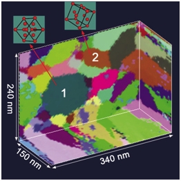
An example of such a 3D map is given in the figure, showing the arrangement of crystals in a 150nm thick nanometal aluminium film. The crystals have identical lattice structure (arrangement of atoms) but they are orientated in different ways in the 3D sample as illustrated by the labels 1 and 2. The colours represent the orientations of the crystals and each crystal is defined by volumes of the same colour. The individual crystals of various sizes (from a few nm to about 100 nm) and shapes (from elongated to spherical) are clearly seen and mapped with a resolution of 1 nanometer.
An important advantage of such 3D methods is that they allow the changes taking place inside a material to be observed directly. For example, the mapping may be repeated before and after a heat treatment revealing how the structure changes during heating.
This new technique has a resolution 100 times better than existing non-destructive 3D techniques and opens up new opportunities for more precise analysis of the structural parameters in nanomaterials.
####
For more information, please click here
Contacts:
Frederiksborgvej 399
P.O.B. 49, 4000 Roskilde
Tel: +45 4677 4677
Fax: +45 4677 5688
Xiaoxu Huang
Senior Scientist
Materials Research (AFM)
Dir tel+45 46775755
Henning Friis Poulsen
Research Professor
Materials Research (AFM)
Dir tel+45 46775739
Sřren Schmidt
Senior Scientist
Materials Research (AFM)
Dir tel+45 46775826
Sřren Schmidt (mobile: 2132 9305)
Xiaoxu Huang (mobile: 2891 4528)
Copyright © Risř DTU
If you have a comment, please Contact us.Issuers of news releases, not 7th Wave, Inc. or Nanotechnology Now, are solely responsible for the accuracy of the content.
Bookmark:


| Related Links |
| Related News Press |
News and information
![]() Quantum computer improves AI predictions April 17th, 2026
Quantum computer improves AI predictions April 17th, 2026
![]() Flexible sensor gains sensitivity under pressure April 17th, 2026
Flexible sensor gains sensitivity under pressure April 17th, 2026
![]() A reusable chip for particulate matter sensing April 17th, 2026
A reusable chip for particulate matter sensing April 17th, 2026
![]() Detecting vibrational quantum beating in the predissociation dynamics of SF6 using time-resolved photoelectron spectroscopy April 17th, 2026
Detecting vibrational quantum beating in the predissociation dynamics of SF6 using time-resolved photoelectron spectroscopy April 17th, 2026
Imaging
![]() Simple algorithm paired with standard imaging tool could predict failure in lithium metal batteries August 8th, 2025
Simple algorithm paired with standard imaging tool could predict failure in lithium metal batteries August 8th, 2025
Discoveries
![]() Quantum computer improves AI predictions April 17th, 2026
Quantum computer improves AI predictions April 17th, 2026
![]() Flexible sensor gains sensitivity under pressure April 17th, 2026
Flexible sensor gains sensitivity under pressure April 17th, 2026
![]() A reusable chip for particulate matter sensing April 17th, 2026
A reusable chip for particulate matter sensing April 17th, 2026
![]() Detecting vibrational quantum beating in the predissociation dynamics of SF6 using time-resolved photoelectron spectroscopy April 17th, 2026
Detecting vibrational quantum beating in the predissociation dynamics of SF6 using time-resolved photoelectron spectroscopy April 17th, 2026
Announcements
![]() A fundamentally new therapeutic approach to cystic fibrosis: Nanobody repairs cellular defect April 17th, 2026
A fundamentally new therapeutic approach to cystic fibrosis: Nanobody repairs cellular defect April 17th, 2026
![]() UC Irvine physicists discover method to reverse ‘quantum scrambling’ : The work addresses the problem of information loss in quantum computing system April 17th, 2026
UC Irvine physicists discover method to reverse ‘quantum scrambling’ : The work addresses the problem of information loss in quantum computing system April 17th, 2026
Research partnerships
![]() Lab to industry: InSe wafer-scale breakthrough for future electronics August 8th, 2025
Lab to industry: InSe wafer-scale breakthrough for future electronics August 8th, 2025
![]() HKU physicists uncover hidden order in the quantum world through deconfined quantum critical points April 25th, 2025
HKU physicists uncover hidden order in the quantum world through deconfined quantum critical points April 25th, 2025
|
|
||
|
|
||
| The latest news from around the world, FREE | ||
|
|
||
|
|
||
| Premium Products | ||
|
|
||
|
Only the news you want to read!
Learn More |
||
|
|
||
|
Full-service, expert consulting
Learn More |
||
|
|
||