Home > Press > Empa researchers use electron beams for chemical reactions: Nanostructures stabilise lasers
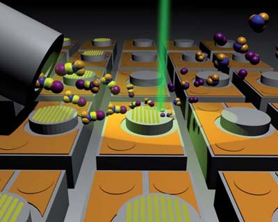 |
| The principle of the local deposition process which is induced with a focussed electron beam (in short, FEBIP): molecules from a gas-injection system are deposited on the sample surface in a reversible manner. The focussed electron beam dissociates adsorbed gas molecules. The resulting non-volatile compounds remain permanently on the sample. |
Abstract:
Electron microscopes use focussed electron beams to make extremely small objects visible. By combining the instrument with a gas-injection system material samples can be manipulated and surface structures measuring only nanometres across can be "written". Empa researchers, together with scientists from EPFL, used this method to improve lasers.
Empa researchers use electron beams for chemical reactions: Nanostructures stabilise lasers
Switzerland | Posted on April 15th, 2011The vertical cavity surface emitting laser (VCSEL) is a semiconductor laser which is often used in data transmission for short-distance links like Gigabit Ethernet. These lasers are very popular in telecommunications because they consume little energy and can be simply fabricated in volumes of many tens of thousands on a single wafer. However, these VCSELs can exhibit one weakness: Because of the cylindrical structure in which the lasers are built up on the wafer, the polarisation of the emitted light can sometimes change during operation. Polarisation is a property of certain waves, such as light waves, and it describes the direction of oscillation. A stable polarisation is necessary in order to reduce transmission errors and to use VCSELs in future silicon photonics.
The team led by Empa researcher Ivo Utke, together with scientists from the Laboratory of Physics of Nanostructures at EPFL, could provide assistance by using a method called FEBIP (focussed electron beam induced processing). "We've written flat grating structures on the VCSELs with an electron beam," says Utke in describing their solution, "and the gratings were effective in stabilising the polarisation." The study has recently been published in the scientific journal "Nanoscale" as an advanced online publication.
Small, minimally invasive, direct
FEBIP is suitable for prototyping nanocomponents, in order to solve specific questions and problems in applied nanoelectronics, nanophotonics and nanobiology. Suitable gas molecules are injected close to a sample which is already in the microscope's vacuum chamber. These adsorb on the sample in a reversible manner. The focussed electron beam, which normally serves to make objects visible, now instead induces chemical reactions of the adsorbed gas molecules, but only at the spot where the beam strikes the surface. The resulting non-volatile molecular fragments then remain permanently on the sample while the volatile fragments are removed by the vacuum system. "With the help of a precisely positioned electron beam, it's possible to remove or apply surface structures with nanometre precision and in virtually any desired three-dimensional shapes," explains Utke.
"FEBIP could soon become a true nanofabrication platform for rapid prototyping of nanostructures in a minimally invasive way, without necessitating the large investment of a clean room."
Book reference
"Nanofabrication using focused ion and electron beams: principles and applications", Editors I. Utke, S. Moshkalev, P. Russels, Oxford Series in Nanomanufacturing. N.Y., Oxford University Press (Nov 2011,), ISBN 9780199734214
####
About Empa
Empa is an interdisciplinary research and services institution for material sciences and technology development within the ETH Domain. Empa�s research and development activities are oriented to meeting the requirements of industry and the needs of our society, and link together applications-oriented research and the practical implementation of new ideas, science and industry, and science and society.
For more information, please click here
Contacts:
* Dr. Ivo Utke
Laboratory for Mechanics of Materials and Nanostructures
Phone +41 33 228 29 57
Redaktion / Medienkontakte
* Beatrice Huber
Communications
Phone +41 58 765 47 33
Copyright © Empa
If you have a comment, please Contact us.Issuers of news releases, not 7th Wave, Inc. or Nanotechnology Now, are solely responsible for the accuracy of the content.
Bookmark:


| Related Links |
| Related News Press |
News and information
![]() Quantum computer improves AI predictions April 17th, 2026
Quantum computer improves AI predictions April 17th, 2026
![]() Flexible sensor gains sensitivity under pressure April 17th, 2026
Flexible sensor gains sensitivity under pressure April 17th, 2026
![]() A reusable chip for particulate matter sensing April 17th, 2026
A reusable chip for particulate matter sensing April 17th, 2026
![]() Detecting vibrational quantum beating in the predissociation dynamics of SF6 using time-resolved photoelectron spectroscopy April 17th, 2026
Detecting vibrational quantum beating in the predissociation dynamics of SF6 using time-resolved photoelectron spectroscopy April 17th, 2026
Imaging
![]() Simple algorithm paired with standard imaging tool could predict failure in lithium metal batteries August 8th, 2025
Simple algorithm paired with standard imaging tool could predict failure in lithium metal batteries August 8th, 2025
![]() First real-time observation of two-dimensional melting process: Researchers at Mainz University unveil new insights into magnetic vortex structures August 8th, 2025
First real-time observation of two-dimensional melting process: Researchers at Mainz University unveil new insights into magnetic vortex structures August 8th, 2025
Chemistry
![]() Projecting light to dispense liquids: A new route to ultra-precise microdroplets January 30th, 2026
Projecting light to dispense liquids: A new route to ultra-precise microdroplets January 30th, 2026
![]() From sensors to smart systems: the rise of AI-driven photonic noses January 30th, 2026
From sensors to smart systems: the rise of AI-driven photonic noses January 30th, 2026
![]() "Nanoreactor" cage uses visible light for catalytic and ultra-selective cross-cycloadditions October 3rd, 2025
"Nanoreactor" cage uses visible light for catalytic and ultra-selective cross-cycloadditions October 3rd, 2025
Laboratories
![]() Researchers develop molecular qubits that communicate at telecom frequencies October 3rd, 2025
Researchers develop molecular qubits that communicate at telecom frequencies October 3rd, 2025
Discoveries
![]() Quantum computer improves AI predictions April 17th, 2026
Quantum computer improves AI predictions April 17th, 2026
![]() Flexible sensor gains sensitivity under pressure April 17th, 2026
Flexible sensor gains sensitivity under pressure April 17th, 2026
![]() A reusable chip for particulate matter sensing April 17th, 2026
A reusable chip for particulate matter sensing April 17th, 2026
![]() Detecting vibrational quantum beating in the predissociation dynamics of SF6 using time-resolved photoelectron spectroscopy April 17th, 2026
Detecting vibrational quantum beating in the predissociation dynamics of SF6 using time-resolved photoelectron spectroscopy April 17th, 2026
Announcements
![]() A fundamentally new therapeutic approach to cystic fibrosis: Nanobody repairs cellular defect April 17th, 2026
A fundamentally new therapeutic approach to cystic fibrosis: Nanobody repairs cellular defect April 17th, 2026
![]() UC Irvine physicists discover method to reverse �quantum scrambling� : The work addresses the problem of information loss in quantum computing system April 17th, 2026
UC Irvine physicists discover method to reverse �quantum scrambling� : The work addresses the problem of information loss in quantum computing system April 17th, 2026
Tools
![]() Metasurfaces smooth light to boost magnetic sensing precision January 30th, 2026
Metasurfaces smooth light to boost magnetic sensing precision January 30th, 2026
![]() From sensors to smart systems: the rise of AI-driven photonic noses January 30th, 2026
From sensors to smart systems: the rise of AI-driven photonic noses January 30th, 2026
![]() Japan launches fully domestically produced quantum computer: Expo visitors to experience quantum computing firsthand August 8th, 2025
Japan launches fully domestically produced quantum computer: Expo visitors to experience quantum computing firsthand August 8th, 2025
Photonics/Optics/Lasers
![]() Metasurfaces smooth light to boost magnetic sensing precision January 30th, 2026
Metasurfaces smooth light to boost magnetic sensing precision January 30th, 2026
![]() From sensors to smart systems: the rise of AI-driven photonic noses January 30th, 2026
From sensors to smart systems: the rise of AI-driven photonic noses January 30th, 2026
|
|
||
|
|
||
| The latest news from around the world, FREE | ||
|
|
||
|
|
||
| Premium Products | ||
|
|
||
|
Only the news you want to read!
Learn More |
||
|
|
||
|
Full-service, expert consulting
Learn More |
||
|
|
||