Home > Press > Getting the Point: Real-Time Monitoring of Atomic-Microscope Probes Adjusts for Wear
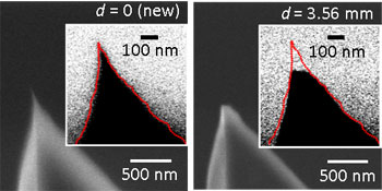 |
| As an atomic force microscope�s tip degrades, the change in tip size and shape affects its resonant frequency and that can be used to accurately measure, in real time, the change in the tip�s shape, thereby resulting in more accurate measurements and images at nanometer size scales. Credit: Jason Killgore, NIST |
Abstract:
Scientists at the National Institute of Standards and Technology (NIST) have developed a way to measure the wear and degradation of the microscopic probes used to study nanoscale structures in situ and as it's happening. Their technique can both dramatically speed up and improve the accuracy of the most precise and delicate nanoscale measurements done with atomic force microscopy (AFM).
Getting the Point: Real-Time Monitoring of Atomic-Microscope Probes Adjusts for Wear
Gaithersburg, MD | Posted on March 31st, 2011If you're trying to measure the contours of a surface with a ruler that's crumbling away as you work, then you at least need to know how fast and to what extent it is being worn away during the measurement.
This has been the challenge for researchers and manufacturers trying to create images of the surfaces of nanomaterials and nanostructures. Taking a photo is impossible at such small scales, so researchers use atomic force microscopes. Think of a device like a phonograph needle being used, on a nanoscale, to measure the peaks and valleys as it's dragged back and forth across a surface. These devices are used extensively in nanoscale imaging to measure the contours of nanostructures, but the AFM tips are so small that they tend to wear down as they traverse the surface being measured.
Today, most researchers stop the measurement to "take a picture" of the tip with an electron microscope, a time-consuming method prone to inaccuracies.
NIST materials engineer Jason Killgore has developed a method for measuring in real time the extent to which AFM tips wear down. Killgore measures the resonant frequency of the AFM sensor tip, a natural vibration rate like that of a tuning fork, while the instrument is in use. Because changes to the size and shape of the tip affect its resonant frequency, he is able to measure the size of the AFM's tip as it works�in increments of a tenth of a nanometer, essentially atomic scale resolution. The technique, called contact resonance force microscopy, is described in a paper recently published in the journal Small.*
The potential impact of this development is considerable. Thousands of AFMs are in use at universities, manufacturing plants and research and development facilities around the world. Improving their ability to measure and image nanosized devices will improve the quality and effectiveness of those devices. Another benefit is that developing new measurement tips�and studying the properties of new materials used in those tips�will be much easier and faster, given the immediate feedback about wear rates.
* J. P. Killgore, R. H. Geiss and D. C. Hurley. Continuous measurement of AFM tip wear by contact resonance force microscopy. Small. Published March 15, 2011.
####
For more information, please click here
Contacts:
James Burrus
303-497-4789
Copyright © NIST
If you have a comment, please Contact us.Issuers of news releases, not 7th Wave, Inc. or Nanotechnology Now, are solely responsible for the accuracy of the content.
Bookmark:


| Related News Press |
News and information
![]() Quantum computer improves AI predictions April 17th, 2026
Quantum computer improves AI predictions April 17th, 2026
![]() Flexible sensor gains sensitivity under pressure April 17th, 2026
Flexible sensor gains sensitivity under pressure April 17th, 2026
![]() A reusable chip for particulate matter sensing April 17th, 2026
A reusable chip for particulate matter sensing April 17th, 2026
![]() Detecting vibrational quantum beating in the predissociation dynamics of SF6 using time-resolved photoelectron spectroscopy April 17th, 2026
Detecting vibrational quantum beating in the predissociation dynamics of SF6 using time-resolved photoelectron spectroscopy April 17th, 2026
Imaging
![]() Simple algorithm paired with standard imaging tool could predict failure in lithium metal batteries August 8th, 2025
Simple algorithm paired with standard imaging tool could predict failure in lithium metal batteries August 8th, 2025
Discoveries
![]() Quantum computer improves AI predictions April 17th, 2026
Quantum computer improves AI predictions April 17th, 2026
![]() Flexible sensor gains sensitivity under pressure April 17th, 2026
Flexible sensor gains sensitivity under pressure April 17th, 2026
![]() A reusable chip for particulate matter sensing April 17th, 2026
A reusable chip for particulate matter sensing April 17th, 2026
![]() Detecting vibrational quantum beating in the predissociation dynamics of SF6 using time-resolved photoelectron spectroscopy April 17th, 2026
Detecting vibrational quantum beating in the predissociation dynamics of SF6 using time-resolved photoelectron spectroscopy April 17th, 2026
Announcements
![]() A fundamentally new therapeutic approach to cystic fibrosis: Nanobody repairs cellular defect April 17th, 2026
A fundamentally new therapeutic approach to cystic fibrosis: Nanobody repairs cellular defect April 17th, 2026
![]() UC Irvine physicists discover method to reverse �quantum scrambling� : The work addresses the problem of information loss in quantum computing system April 17th, 2026
UC Irvine physicists discover method to reverse �quantum scrambling� : The work addresses the problem of information loss in quantum computing system April 17th, 2026
Tools
![]() Metasurfaces smooth light to boost magnetic sensing precision January 30th, 2026
Metasurfaces smooth light to boost magnetic sensing precision January 30th, 2026
![]() From sensors to smart systems: the rise of AI-driven photonic noses January 30th, 2026
From sensors to smart systems: the rise of AI-driven photonic noses January 30th, 2026
![]() Japan launches fully domestically produced quantum computer: Expo visitors to experience quantum computing firsthand August 8th, 2025
Japan launches fully domestically produced quantum computer: Expo visitors to experience quantum computing firsthand August 8th, 2025
|
|
||
|
|
||
| The latest news from around the world, FREE | ||
|
|
||
|
|
||
| Premium Products | ||
|
|
||
|
Only the news you want to read!
Learn More |
||
|
|
||
|
Full-service, expert consulting
Learn More |
||
|
|
||