Home > Press > Berkeley Lab Researchers Create Next-Generation Chemical Mapping on the Nanoscale
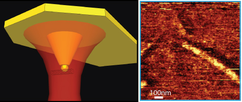 |
| Schematic of coaxial probe for imaging a carbon nanotube (left) and chemical map of carbon nanotube with chemical and topographical information at each pixel (right). |
Abstract:
A pixel is worth a thousand words? Not exactly how the saying goes, but in this case, it holds true: scientists at Berkeley Lab's Molecular Foundry have pioneered a new chemical mapping method that provides unprecedented insight into materials at the nanoscale. Moving beyond traditional static imaging techniques, which provide a snapshot in time, these new maps will guide researchers in deciphering molecular chemistry and interactions at the nanoscale—critical for artificial photosynthesis, biofuels production and light-harvesting applications such as solar cells.
Berkeley Lab Researchers Create Next-Generation Chemical Mapping on the Nanoscale
Berkeley, CA | Posted on March 28th, 2011"This new technique allows us to capture very high-resolution images of nanomaterials with a huge amount of physical and chemical information at each pixel," says Alexander Weber-Bargioni, a postdoctoral scholar in the Imaging and Manipulation of Nanostructures Facility at the Foundry. "Usually when you take an image, you just get a picture of what this material looks like, but nothing more. With our method, we can now gain information about the functionality of a nanostructure with rich detail."
The Molecular Foundry is a U.S. Department of Energy (DOE) Office of Science nanoscience center and national user facility. With the Foundry's state-of-the-art focused ion beam tool at their disposal, Weber-Bargioni and his team designed and fabricated a coaxial antenna capable of focusing light at the nanoscale, - a harnessing of light akin to wielding a sharp knife in a thunderstorm, Weber-Bargioni says.
Consisting of gold wrapped around a silicon nitride atomic force microscope tip, this coaxial antenna serves as an optical probe for structures with nanometer resolution for several hours at a time. What's more, unlike other scanning probe tips, it provides enough enhancement, or light intensity, to report the chemical fingerprint at each pixel while collecting an image (typically 256 x 256 pixels). This data is then used to generate multiple composition-related "maps," each with a wealth of chemical information at every pixel, at a resolution of just twenty nanometers. The maps provide information that is critical for examining nanomaterials, in which local surface chemistry and interfaces dominate behavior.
"Fabricating reproducible near-field optical microscopy probes has always been a challenge," says Frank Ogletree, acting Facility Director of the Imaging and Manipulation of Nanostructures Facility at the Foundry. "We now have a high-yield method to make engineered plasmonic probes for spectroscopy on a variety of surfaces."
To test out the capability of their new probe, the team examined carbon nanotubes, sheets of carbon atoms rolled tightly into tubes just a few nanometers in diameter. Carbon nanotubes are ideal for this type of interactive investigation as their unmatched electronic and structural properties are sensitive to localized chemical changes.
Users coming to the Molecular Foundry to seek information about light-harvesting materials or any dynamic system should benefit from this imaging system, Weber-Bargioni says.
Adds Jim Schuck, staff scientist in the Imaging and Manipulation of Nanostructures Facility at the Foundry, "We're very excited—this new nano-optics capability enables us to explore previously inaccessible properties within nanosystems. The work reflects a major strength of the Molecular Foundry, where collaboration between scientists with complementary expertise leads to real nanoscience breakthroughs."
A paper reporting this research titled, "Hyperspectral nanoscale imaging on dielectric substrates with coaxial optical antenna scan probes," appears in Nano Letters and is available to subscribers online. Co-authoring the paper with Weber-Bargioni, Ogletree and Schuck were Adam Schwartzberg, Matteo Cornaglia, Ariel Ismach, Jeffrey Urban, Yuanjie Pang, Reuven Gordon, Jeffrey Bokor, Miquel Salmeron, Paul Ashby and Stefano Cabrini.
This work at the Molecular Foundry was supported by DOE's Office of Science.
The Molecular Foundry is one of the five DOE Nanoscale Science Research Centers (NSRCs), national user facilities for interdisciplinary research at the nanoscale, supported by the DOE Office of Science. Together the NSRCs comprise a suite of complementary facilities that provide researchers with state-of-the-art capabilities to fabricate, process, characterize and model nanoscale materials, and constitute the largest infrastructure investment of the National Nanotechnology Initiative. The NSRCs are located at DOE's Argonne, Brookhaven, Lawrence Berkeley, Oak Ridge and Sandia and Los Alamos National Laboratories. For more information about the DOE NSRCs, please visit http://nano.energy.gov.
####
About Berkeley Lab
Lawrence Berkeley National Laboratory is a U.S. Department of Energy (DOE) national laboratory managed by the University of California for the DOE Office of Science. Berkeley Lab provides solutions to the world’s most urgent scientific challenges including sustainable energy, climate change, human health, and a better understanding of matter and force in the universe. It is a world leader in improving our lives through team science, advanced computing, and innovative technology.
For more information, please click here
Contacts:
Aditi Risbud
(510)486-4861
Copyright © Berkeley Lab
If you have a comment, please Contact us.Issuers of news releases, not 7th Wave, Inc. or Nanotechnology Now, are solely responsible for the accuracy of the content.
Bookmark:


| Related News Press |
Chemistry
![]() Projecting light to dispense liquids: A new route to ultra-precise microdroplets January 30th, 2026
Projecting light to dispense liquids: A new route to ultra-precise microdroplets January 30th, 2026
![]() From sensors to smart systems: the rise of AI-driven photonic noses January 30th, 2026
From sensors to smart systems: the rise of AI-driven photonic noses January 30th, 2026
![]() "Nanoreactor" cage uses visible light for catalytic and ultra-selective cross-cycloadditions October 3rd, 2025
"Nanoreactor" cage uses visible light for catalytic and ultra-selective cross-cycloadditions October 3rd, 2025
![]() Cambridge chemists discover simple way to build bigger molecules – one carbon at a time June 6th, 2025
Cambridge chemists discover simple way to build bigger molecules – one carbon at a time June 6th, 2025
![]() Single-atom catalysts change spin state when boosted by a magnetic field June 4th, 2025
Single-atom catalysts change spin state when boosted by a magnetic field June 4th, 2025
Laboratories
![]() Researchers develop molecular qubits that communicate at telecom frequencies October 3rd, 2025
Researchers develop molecular qubits that communicate at telecom frequencies October 3rd, 2025
Govt.-Legislation/Regulation/Funding/Policy
![]() Quantum computer improves AI predictions April 17th, 2026
Quantum computer improves AI predictions April 17th, 2026
![]() Metasurfaces smooth light to boost magnetic sensing precision January 30th, 2026
Metasurfaces smooth light to boost magnetic sensing precision January 30th, 2026
![]() New imaging approach transforms study of bacterial biofilms August 8th, 2025
New imaging approach transforms study of bacterial biofilms August 8th, 2025
Nanotubes/Buckyballs/Fullerenes/Nanorods/Nanostrings/Nanosheets
![]() Tiny nanosheets, big leap: A new sensor detects ethanol at ultra-low levels January 30th, 2026
Tiny nanosheets, big leap: A new sensor detects ethanol at ultra-low levels January 30th, 2026
![]() Enhancing power factor of p- and n-type single-walled carbon nanotubes April 25th, 2025
Enhancing power factor of p- and n-type single-walled carbon nanotubes April 25th, 2025
![]() Chainmail-like material could be the future of armor: First 2D mechanically interlocked polymer exhibits exceptional flexibility and strength January 17th, 2025
Chainmail-like material could be the future of armor: First 2D mechanically interlocked polymer exhibits exceptional flexibility and strength January 17th, 2025
![]() Innovative biomimetic superhydrophobic coating combines repair and buffering properties for superior anti-erosion December 13th, 2024
Innovative biomimetic superhydrophobic coating combines repair and buffering properties for superior anti-erosion December 13th, 2024
Discoveries
![]() Quantum computer improves AI predictions April 17th, 2026
Quantum computer improves AI predictions April 17th, 2026
![]() Flexible sensor gains sensitivity under pressure April 17th, 2026
Flexible sensor gains sensitivity under pressure April 17th, 2026
![]() A reusable chip for particulate matter sensing April 17th, 2026
A reusable chip for particulate matter sensing April 17th, 2026
![]() Detecting vibrational quantum beating in the predissociation dynamics of SF6 using time-resolved photoelectron spectroscopy April 17th, 2026
Detecting vibrational quantum beating in the predissociation dynamics of SF6 using time-resolved photoelectron spectroscopy April 17th, 2026
Announcements
![]() A fundamentally new therapeutic approach to cystic fibrosis: Nanobody repairs cellular defect April 17th, 2026
A fundamentally new therapeutic approach to cystic fibrosis: Nanobody repairs cellular defect April 17th, 2026
![]() UC Irvine physicists discover method to reverse ‘quantum scrambling’ : The work addresses the problem of information loss in quantum computing system April 17th, 2026
UC Irvine physicists discover method to reverse ‘quantum scrambling’ : The work addresses the problem of information loss in quantum computing system April 17th, 2026
Energy
![]() Sensors innovations for smart lithium-based batteries: advancements, opportunities, and potential challenges August 8th, 2025
Sensors innovations for smart lithium-based batteries: advancements, opportunities, and potential challenges August 8th, 2025
![]() Simple algorithm paired with standard imaging tool could predict failure in lithium metal batteries August 8th, 2025
Simple algorithm paired with standard imaging tool could predict failure in lithium metal batteries August 8th, 2025
New-Contracts/Sales/Customers
![]() Bruker Light-Sheet Microscopes at Major Comprehensive Cancer Center: New Advanced Imaging Center Powered by Two MuVi and LCS SPIM Microscopes March 25th, 2021
Bruker Light-Sheet Microscopes at Major Comprehensive Cancer Center: New Advanced Imaging Center Powered by Two MuVi and LCS SPIM Microscopes March 25th, 2021
![]() Arrowhead Pharmaceuticals Announces Closing of Agreement with Takeda November 27th, 2020
Arrowhead Pharmaceuticals Announces Closing of Agreement with Takeda November 27th, 2020
![]() Veeco Announces Aledia Order of 300mm MOCVD Equipment for microLED Displays: Propel™ Platform First 300mm System with EFEM Designed for Advanced Display Applications October 20th, 2020
Veeco Announces Aledia Order of 300mm MOCVD Equipment for microLED Displays: Propel™ Platform First 300mm System with EFEM Designed for Advanced Display Applications October 20th, 2020
![]() GREENWAVES TECHNOLOGIES Announces Next Generation GAP9 Hearables Platform Using GLOBALFOUNDRIES 22FDX Solution October 16th, 2020
GREENWAVES TECHNOLOGIES Announces Next Generation GAP9 Hearables Platform Using GLOBALFOUNDRIES 22FDX Solution October 16th, 2020
Solar/Photovoltaic
![]() Spinel-type sulfide semiconductors to operate the next-generation LEDs and solar cells For solar-cell absorbers and green-LED source October 3rd, 2025
Spinel-type sulfide semiconductors to operate the next-generation LEDs and solar cells For solar-cell absorbers and green-LED source October 3rd, 2025
![]() KAIST researchers introduce new and improved, next-generation perovskite solar cell November 8th, 2024
KAIST researchers introduce new and improved, next-generation perovskite solar cell November 8th, 2024
![]() Groundbreaking precision in single-molecule optoelectronics August 16th, 2024
Groundbreaking precision in single-molecule optoelectronics August 16th, 2024
![]() Development of zinc oxide nanopagoda array photoelectrode: photoelectrochemical water-splitting hydrogen production January 12th, 2024
Development of zinc oxide nanopagoda array photoelectrode: photoelectrochemical water-splitting hydrogen production January 12th, 2024
|
|
||
|
|
||
| The latest news from around the world, FREE | ||
|
|
||
|
|
||
| Premium Products | ||
|
|
||
|
Only the news you want to read!
Learn More |
||
|
|
||
|
Full-service, expert consulting
Learn More |
||
|
|
||