Home > Press > Sarfus 3D-IMM: New equipement for nanometric sample charaterization in water
 |
Abstract:
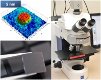
Nanolane is proud to announce the launch of its new equipment SARFUS 3D-IMM dedicated to the topographic characterization of nanometric samples in water.
Sarfus 3D-IMM: New equipement for nanometric sample charaterization in water
France | Posted on September 6th, 2010Equipments for characterization in water are still rare, relatively complex to operate and do not offer real-time images of samples. SARFUS 3D-IMM is designed to match the needs of the engineering and research community, especially in the Life Science but also in Thin Film and Surface Treatment areas. Indeed, SARFUS 3D-IMM is dedicated to the observation of nano-objects in real-time and to the thickness measurements of ultra-thin films in water.
Like the other SARFUS products, SARFUS 3D-IMM is based on SEEC optical technique that uses specific nonreflecting surfaces for cross-polarized reflected light microscopy. These surfaces -the Surfs- are used instead of standard microscope slides and generate a contrast enhancement of about 2 orders of magnitude, extending the application fields of optical microscopy toward the nanoworld.
Thanks to the absence of scanning and its easiness of use, SARFUS 3D-IMM equipment opens new perspectives for the nano-characterization in aqueous media by allowing dynamic studies of nanometric structures and rapid quality control of samples. In addition, the equipment is proposed with a powerful 3D topographic software for complete characterization (layer thicknesses, section profiles, roughnesses...) of nanometric samples.
The main applications concerned by this innovation are:
Biological objets
- Vesicles
- Lipid bilayers
- Biochips
- Cell adhesion
- ...
Thin films & Surface Treatment
- Polyelectrolytes
- Sensitive films (LCST)
- Nano-films
- Polymer patterns
- ...
The main features of SARFUS 3D-IMM equipment are:
- User friendly & Fast processing
- Repeatability : 0.1nm (according to ISO standard 17025)
- Z-sensibility limit: 0.2nm
- Range of measurement: 1 to 60nm
- Lateral resolution : 330nm
- Live video acquisition
- Time lapse (up to 15 image per second)
- Non destructive, no labelling
- Compatibility with fluorescence
####
About �olane
�olane is the signature, of seven companies, all gathered under 100% control of a holding, the �Financi�re de l�Ombr�e�, whose main activity is the conception, the study and the manufacture of professional electronic materials.
Each of them operates in complementary fields (technologies, industrial resource, economic sectors, and geographical areas). Strong synergies are present between them (conception, purchases, sales, industry, networks, and quality, to quote only the principal ones).
For more information, please click here
Contacts:
Nicolas Medard
Copyright © �olane
If you have a comment, please Contact us.Issuers of news releases, not 7th Wave, Inc. or Nanotechnology Now, are solely responsible for the accuracy of the content.
Bookmark:


| Related News Press |
News and information
![]() Quantum computer improves AI predictions April 17th, 2026
Quantum computer improves AI predictions April 17th, 2026
![]() Flexible sensor gains sensitivity under pressure April 17th, 2026
Flexible sensor gains sensitivity under pressure April 17th, 2026
![]() A reusable chip for particulate matter sensing April 17th, 2026
A reusable chip for particulate matter sensing April 17th, 2026
![]() Detecting vibrational quantum beating in the predissociation dynamics of SF6 using time-resolved photoelectron spectroscopy April 17th, 2026
Detecting vibrational quantum beating in the predissociation dynamics of SF6 using time-resolved photoelectron spectroscopy April 17th, 2026
Thin films
![]() Tiny nanosheets, big leap: A new sensor detects ethanol at ultra-low levels January 30th, 2026
Tiny nanosheets, big leap: A new sensor detects ethanol at ultra-low levels January 30th, 2026
![]() Utilizing palladium for addressing contact issues of buried oxide thin film transistors April 5th, 2024
Utilizing palladium for addressing contact issues of buried oxide thin film transistors April 5th, 2024
![]() Understanding the mechanism of non-uniform formation of diamond film on tools: Paving the way to a dry process with less environmental impact March 24th, 2023
Understanding the mechanism of non-uniform formation of diamond film on tools: Paving the way to a dry process with less environmental impact March 24th, 2023
![]() New study introduces the best graphite films: The work by Distinguished Professor Feng Ding at UNIST has been published in the October 2022 issue of Nature Nanotechnology November 4th, 2022
New study introduces the best graphite films: The work by Distinguished Professor Feng Ding at UNIST has been published in the October 2022 issue of Nature Nanotechnology November 4th, 2022
Announcements
![]() A fundamentally new therapeutic approach to cystic fibrosis: Nanobody repairs cellular defect April 17th, 2026
A fundamentally new therapeutic approach to cystic fibrosis: Nanobody repairs cellular defect April 17th, 2026
![]() UC Irvine physicists discover method to reverse �quantum scrambling� : The work addresses the problem of information loss in quantum computing system April 17th, 2026
UC Irvine physicists discover method to reverse �quantum scrambling� : The work addresses the problem of information loss in quantum computing system April 17th, 2026
Tools
![]() Metasurfaces smooth light to boost magnetic sensing precision January 30th, 2026
Metasurfaces smooth light to boost magnetic sensing precision January 30th, 2026
![]() From sensors to smart systems: the rise of AI-driven photonic noses January 30th, 2026
From sensors to smart systems: the rise of AI-driven photonic noses January 30th, 2026
![]() Japan launches fully domestically produced quantum computer: Expo visitors to experience quantum computing firsthand August 8th, 2025
Japan launches fully domestically produced quantum computer: Expo visitors to experience quantum computing firsthand August 8th, 2025
|
|
||
|
|
||
| The latest news from around the world, FREE | ||
|
|
||
|
|
||
| Premium Products | ||
|
|
||
|
Only the news you want to read!
Learn More |
||
|
|
||
|
Full-service, expert consulting
Learn More |
||
|
|
||