Home > Press > New ISO methodology demystifies nanomaterials
 |
Abstract:
From new medical applications, to the latest gadgets and consumer products, innovative nanotechnology is pushing the boundaries of what we believed possible. But for this technology to develop further, faster and better we need a clear understanding and a logical classification of nanomaterials.
New ISO methodology demystifies nanomaterials
Switzerland | Posted on August 27th, 2010ISO has therefore published a new technical report, ISO/TR 11360:2010, Nanotechnologies - Methodology for the classification and categorization of nanomaterials, offering a comprehensive, globally harmonized methodology for classifying nanomaterials.
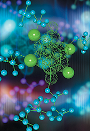
Nanotechnology deals with structures between 1 to 100 nanometers. Applications are wide, and range from computer memory storage to sunscreens. Nanomaterials currently in existence exhibit various physical, chemical, mechanical, optical, magnetic and biological properties, as well as different internal/external structures.
Because scientists and researches in this new field have very diverse backgrounds, and are working on different applications, there are now many divergent understandings and assumptions associated with emerging scientific concepts in this area. This is causing poor communication, lack of interoperability among systems and duplication of efforts.
ISO/TR 11360 introduces a system called the "nano-tree", which places nanotechnology concepts into a logical context by indicating relationships among them as a branching out tree. The most basic and common elements are defined as the main trunk of the tree, and nanomaterials are then differentiated in terms of structure, chemical nature and other properties.
"The document provides users with a structured view of nanotechnology, and facilitates a common understanding of its concepts," says Peter Hatto, Chair of the committee that developed the standard (ISO/TC 229). "It offers a systematic approach and a commonsensical hierarchy".
Dr. Hatto adds, "The benefits for this emerging field are enormous. Most importantly, ISO/TR 11360 will promote clear and useful communication amongst industry consumers, governments and regulatory bodies".
The document will be useful to a wide range of scientific and engineering disciplines engaged in research, industry and government.
ISO/TR 11360:2010, Nanotechnologies - Methodology for the classification and categorization of nanomaterials, was developed ISO technical committee ISO/TC 229, Nanotechologies, and is available from ISO national member institutes (see the complete list with contact details). It may also be obtained directly from the ISO Central Secretariat, price 112 Swiss francs through the ISO Store or by contacting the Marketing, Communication & Information department.
####
About ISO
ISO (International Organization for Standardization) is the world's largest developer and publisher of International Standards.
ISO is a network of the national standards institutes of 163 countries, one member per country, with a Central Secretariat in Geneva, Switzerland, that coordinates the system.
ISO is a non-governmental organization that forms a bridge between the public and private sectors. On the one hand, many of its member institutes are part of the governmental structure of their countries, or are mandated by their government. On the other hand, other members have their roots uniquely in the private sector, having been set up by national partnerships of industry associations.
Therefore, ISO enables a consensus to be reached on solutions that meet both the requirements of business and the broader needs of society.
For more information, please click here
Contacts:
Sales:
Mrs. Sonia Rosas Friot
Assistant, Marketing Services
Marketing, Communication and Information
Tel. +41 22 749 03 36
Fax +41 22 749 09 47
Maria Lazarte
Communication Officer,
Marketing, Communication and Information
Tel. +41 22 749 01 11
Fax +41 22 733 34 30
Copyright © ISO
If you have a comment, please Contact us.Issuers of news releases, not 7th Wave, Inc. or Nanotechnology Now, are solely responsible for the accuracy of the content.
Bookmark:


| Related News Press |
News and information
![]() Quantum computer improves AI predictions April 17th, 2026
Quantum computer improves AI predictions April 17th, 2026
![]() Flexible sensor gains sensitivity under pressure April 17th, 2026
Flexible sensor gains sensitivity under pressure April 17th, 2026
![]() A reusable chip for particulate matter sensing April 17th, 2026
A reusable chip for particulate matter sensing April 17th, 2026
![]() Detecting vibrational quantum beating in the predissociation dynamics of SF6 using time-resolved photoelectron spectroscopy April 17th, 2026
Detecting vibrational quantum beating in the predissociation dynamics of SF6 using time-resolved photoelectron spectroscopy April 17th, 2026
Govt.-Legislation/Regulation/Funding/Policy
![]() Quantum computer improves AI predictions April 17th, 2026
Quantum computer improves AI predictions April 17th, 2026
![]() Metasurfaces smooth light to boost magnetic sensing precision January 30th, 2026
Metasurfaces smooth light to boost magnetic sensing precision January 30th, 2026
![]() New imaging approach transforms study of bacterial biofilms August 8th, 2025
New imaging approach transforms study of bacterial biofilms August 8th, 2025
Materials/Metamaterials/Magnetoresistance
![]() First real-time observation of two-dimensional melting process: Researchers at Mainz University unveil new insights into magnetic vortex structures August 8th, 2025
First real-time observation of two-dimensional melting process: Researchers at Mainz University unveil new insights into magnetic vortex structures August 8th, 2025
![]() Researchers unveil a groundbreaking clay-based solution to capture carbon dioxide and combat climate change June 6th, 2025
Researchers unveil a groundbreaking clay-based solution to capture carbon dioxide and combat climate change June 6th, 2025
![]() A 1960s idea inspires NBI researchers to study hitherto inaccessible quantum states June 6th, 2025
A 1960s idea inspires NBI researchers to study hitherto inaccessible quantum states June 6th, 2025
![]() Institute for Nanoscience hosts annual proposal planning meeting May 16th, 2025
Institute for Nanoscience hosts annual proposal planning meeting May 16th, 2025
Announcements
![]() A fundamentally new therapeutic approach to cystic fibrosis: Nanobody repairs cellular defect April 17th, 2026
A fundamentally new therapeutic approach to cystic fibrosis: Nanobody repairs cellular defect April 17th, 2026
![]() UC Irvine physicists discover method to reverse �quantum scrambling� : The work addresses the problem of information loss in quantum computing system April 17th, 2026
UC Irvine physicists discover method to reverse �quantum scrambling� : The work addresses the problem of information loss in quantum computing system April 17th, 2026
Interviews/Book Reviews/Essays/Reports/Podcasts/Journals/White papers/Posters
![]() A fundamentally new therapeutic approach to cystic fibrosis: Nanobody repairs cellular defect April 17th, 2026
A fundamentally new therapeutic approach to cystic fibrosis: Nanobody repairs cellular defect April 17th, 2026
![]() UC Irvine physicists discover method to reverse �quantum scrambling� : The work addresses the problem of information loss in quantum computing system April 17th, 2026
UC Irvine physicists discover method to reverse �quantum scrambling� : The work addresses the problem of information loss in quantum computing system April 17th, 2026
|
|
||
|
|
||
| The latest news from around the world, FREE | ||
|
|
||
|
|
||
| Premium Products | ||
|
|
||
|
Only the news you want to read!
Learn More |
||
|
|
||
|
Full-service, expert consulting
Learn More |
||
|
|
||