Home > Press > Spartanics Announces On-Site Nanomaterials Testing For Laser Die Cutting During 2010/2011 Worldwide Trade Events
 |
Abstract:
Nanomaterials engineers will be able to obtain immediate on-site no-cost materials analyses of suitability for finishing, marking and other detailing with laser die cutting from Spartanics Laser Die Cutting Materials Applications Laboratory (1) engineers attending a series of worldwide trade events in the coming year (1). Nanomaterials engineers are invited to bring samples to these various events, and for many to also obtain free passes to the events from Spartanics.
Spartanics Announces On-Site Nanomaterials Testing For Laser Die Cutting During 2010/2011 Worldwide Trade Events
Rolling Meadows, IL | Posted on June 15th, 2010The first scheduled event is Label Expo Americas 2010 (2) to be held in Suburban Chicago, Illinois, USA on September 14 - 16, 2010. Passes for this event can be obtained by writing to Sharon Bagby, Spartanics Marketing Coordinator,
The full schedule for the mobile Spartanics Laser Die Cutting Applications Laboratory for Materials Research events will be announced in the coming months. Preliminary inquiries can be directed to Mike Bacon, Spartanics VP,
Spartanics laser die cutting applications engineers have extensively tested laser die cutters with varying laser strengths and software configurations with a wide range of materials including: plastic films, polyesters, polycarbonates, foams, textiles, paper, adhesive tapes, non-wovens, wood, laminates, pressure-sensitive substrates, magnetic materials, polypropylene, polymides, abrasives, rubber, among others. Formalization of the Applications Laboratory signals Spartanics intent to systematize this growing knowledgebase for cross-industry access.
The Mobile Spartanics Laser Die Cutting Applications Laboratory for Materials Research (1) will provide no-cost detailed engineering analyses of maximum material thicknesses that can be handled with these different substrates, including brand name materials, correlated to laser power and other variables.
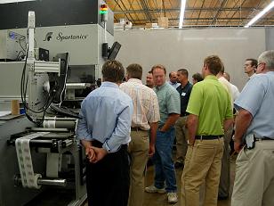
Spartanics Finecut Laser Die Cutting Systems (3)--sheet, roll or combination sheet/roll-- are used in a wide array of applications --- flexible circuits, membrane switches, gaskets, labels, cardstock and paperboard products, packaging, automotive and medical device components, discs, belts, and gaskets, novelty magnets, RFID tags, P-O-P display products, industrial textile applications, and more. Video demonstrations of Spartanics Finecut technology can be seen at www.spartanics.com/index.cgi?videoid=2 .
(1) www.spartanics.com/products_detail.cgi?id_num=59&styleid=2
(2) www.spartanics.com/events_detail.cgi?id_num=22
(3) www.spartanics.com/product_groups_detail.cgi?id_num=5
####
About Spartanics
Spartanics (www.spartanics.com) specializes in tightly integrating advanced software engineering with sophisticated handling systems to manufacture best-in-class technology for both tool-free (laser-based), steel rule die, and male/female hard tool cutting systems, screen printing systems and other equipment for fabricating products made from flat stock materials. Its worldwide service organization uses state-of-the-art virtual service technician technology and also maintains offices and spare parts in Europe.
For more information, please click here
Contacts:
Sales inquiries can be directed to +847-394-5700.
Amy Munice
ALM Communications
+1-773-862-6800
Copyright © Spartanics
If you have a comment, please Contact us.Issuers of news releases, not 7th Wave, Inc. or Nanotechnology Now, are solely responsible for the accuracy of the content.
Bookmark:


| Related News Press |
News and information
![]() Quantum computer improves AI predictions April 17th, 2026
Quantum computer improves AI predictions April 17th, 2026
![]() Flexible sensor gains sensitivity under pressure April 17th, 2026
Flexible sensor gains sensitivity under pressure April 17th, 2026
![]() A reusable chip for particulate matter sensing April 17th, 2026
A reusable chip for particulate matter sensing April 17th, 2026
![]() Detecting vibrational quantum beating in the predissociation dynamics of SF6 using time-resolved photoelectron spectroscopy April 17th, 2026
Detecting vibrational quantum beating in the predissociation dynamics of SF6 using time-resolved photoelectron spectroscopy April 17th, 2026
Materials/Metamaterials/Magnetoresistance
![]() First real-time observation of two-dimensional melting process: Researchers at Mainz University unveil new insights into magnetic vortex structures August 8th, 2025
First real-time observation of two-dimensional melting process: Researchers at Mainz University unveil new insights into magnetic vortex structures August 8th, 2025
![]() Researchers unveil a groundbreaking clay-based solution to capture carbon dioxide and combat climate change June 6th, 2025
Researchers unveil a groundbreaking clay-based solution to capture carbon dioxide and combat climate change June 6th, 2025
![]() A 1960s idea inspires NBI researchers to study hitherto inaccessible quantum states June 6th, 2025
A 1960s idea inspires NBI researchers to study hitherto inaccessible quantum states June 6th, 2025
![]() Institute for Nanoscience hosts annual proposal planning meeting May 16th, 2025
Institute for Nanoscience hosts annual proposal planning meeting May 16th, 2025
Announcements
![]() A fundamentally new therapeutic approach to cystic fibrosis: Nanobody repairs cellular defect April 17th, 2026
A fundamentally new therapeutic approach to cystic fibrosis: Nanobody repairs cellular defect April 17th, 2026
![]() UC Irvine physicists discover method to reverse �quantum scrambling� : The work addresses the problem of information loss in quantum computing system April 17th, 2026
UC Irvine physicists discover method to reverse �quantum scrambling� : The work addresses the problem of information loss in quantum computing system April 17th, 2026
Tools
![]() Metasurfaces smooth light to boost magnetic sensing precision January 30th, 2026
Metasurfaces smooth light to boost magnetic sensing precision January 30th, 2026
![]() From sensors to smart systems: the rise of AI-driven photonic noses January 30th, 2026
From sensors to smart systems: the rise of AI-driven photonic noses January 30th, 2026
![]() Japan launches fully domestically produced quantum computer: Expo visitors to experience quantum computing firsthand August 8th, 2025
Japan launches fully domestically produced quantum computer: Expo visitors to experience quantum computing firsthand August 8th, 2025
Events/Classes
![]() Institute for Nanoscience hosts annual proposal planning meeting May 16th, 2025
Institute for Nanoscience hosts annual proposal planning meeting May 16th, 2025
![]() A New Blue: Mysterious origin of the ribbontail ray�s electric blue spots revealed July 5th, 2024
A New Blue: Mysterious origin of the ribbontail ray�s electric blue spots revealed July 5th, 2024
![]() Researchers demonstrate co-propagation of quantum and classical signals: Study shows that quantum encryption can be implemented in existing fiber networks January 20th, 2023
Researchers demonstrate co-propagation of quantum and classical signals: Study shows that quantum encryption can be implemented in existing fiber networks January 20th, 2023
|
|
||
|
|
||
| The latest news from around the world, FREE | ||
|
|
||
|
|
||
| Premium Products | ||
|
|
||
|
Only the news you want to read!
Learn More |
||
|
|
||
|
Full-service, expert consulting
Learn More |
||
|
|
||