Home > Press > Berkeley Researchers Take the Lead Out of Piezoelectrics
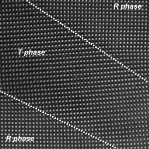 |
| This high-resolution electron micrograph shows the the boundaries between rhombohedral (R phase) and tetragonal (T phase) regions � indicated by dashed lines - in a thin film of bismuth ferrite under epitaxial strain. A smooth transition between phases is observed with no dislocations or defects at the interface. The image was produced on TEAM 0.5 at the National Center for Electron Microscopy. |
Abstract:
By applying just the right compression to thin films of bismuth ferrite, Berkeley Lab researchers have produced a lead-free alternative to the current crop of piezoelectric materials.
Berkeley Researchers Take the Lead Out of Piezoelectrics
Berkeley, CA | Posted on November 25th, 2009There is good news for the global effort to reduce the amount of lead in the environment and for the growing array of technologies that rely upon the piezoelectric effect. A lead-free alternative to the current crop of piezoelectric materials has been identified by researchers with the U.S. Department of Energy's Lawrence Berkeley National Laboratory (Berkeley Lab) and the University of California (UC), Berkeley.
The key to this success is the use of bismuth ferrite, a compound with a perovskite crystal structure, meaning it has crystal planes of oxygen and bismuth atoms alternating with planes of oxygen and iron atoms. These planes can move relative to one other when the proper strain is applied. The research team discovered that the piezoelectric effect in bismuth ferrite becomes significantly enhanced in response to the application of epitaxial strain -compression in the direction of its crystal planes.
"We have demonstrated that epitaxial strain can be used to create a large piezoelectric responses in thin films of bismuth ferrite," says Ramamoorthy Ramesh, a materials scientist who led this research. "The piezoelectric effect is reversible when the strain is relaxed."
Ramesh holds joint appointments with Berkeley Lab's Materials Sciences Division and UC Berkeley's Department of Materials Science and Engineering and the Department of Physics. He is the senior author on a paper published in the journal Science entitled: "A Strain-Driven Morphotropic Phase Boundary in BiFeO3."
Co-authoring the paper with Ramesh were Robert Zeches, Marta-Dacil Rossell, Jinxing Zhang, Alison Hatt, Qing He, Chan-Ho Yang, Amit Kumar, Chih-Hubng Wang, Alexander Melville, Carolina Adamo, Guang Sheng, Ying-Hao Chu, Jon Ihlefeld, Rolf Erni, Claude Ederer, Venkatraman Gopalan, Long-Qing Chen, Darrell Schlom, Nicola Spaldin and Lane Martin.
"In principle, the strain-driven piezoelectric effect we have observed in bismuth ferrite should be generic to other lead-free perovskites as well," Ramesh says, "akin to chemically driven effects that are now well established in the manganites, cuprates and relaxors."
Piezoelectric materials, as a result of their unique crystal structures, are able to couple mechanical and electrical properties. Place a mechanical strain on a piezoelectric and an electric charge is generated across its surface. Subject a piezoelectric to an electric charge and its shape becomes deformed. The electromechanical properties of piezoelectric materials have made them valuable components in a broad range of devices, including sensors, actuators and transducers. They are especially valuable for medical ultrasounds and for non-destructive testing of roads and bridges.
The most widely used piezoelectric materials today are lead-based perovskite compounds, especially lead zirconate titanate (PZT). These perovskites display superior piezoelectric properties in areas where the phase of their crystal structure abruptly changes. Such areas, known as morphotropic phase boundaries, are produced via complex chemical alloying of a PZT-type perovskite's metal and oxide constituents. While the technology is well established, lead is a potent neurotoxin that poses a serious threat to human health, especially children, and to the environment.
"We have produced the piezoelectric effect by taking thin films of bismuth ferrite and applying a huge epitaxial strain," says Robert Zeches, a member of Ramesh's UC Berkeley research group who was the first author on the Science paper. "The bismuth ferrite wants to be in a rhombohedral phase but the epitaxial strain forces it into a tetragonal phase, creating a morphotropic phase boundary."
If the strain is removed, the bismuth ferrite crystal structure reverts back to its original rhombohedral-like phase, Zeches says. By alternating between squeezing and relaxing, the researchers can shuttle the material back and forth between the two phases.
Ramesh joking observed that, "Inducing materials into such a schizophrenic state can be the key to obtaining exotic behavior."
Ramesh and his group are now testing their strain-driven piezoelectric technique on other perovskites. They are also exploring the use of epitaxial strain to generate other phenomena such as magnetoresistance. Noting that the reversible phase changes in the bismuth ferrite films are accompanied by changes of a few nanometers in the height of the sample surface - a substantial change on this scale - Ramesh and his colleagues believe their results make bismuth ferrite an attractive candidate for data storage applications.
The bismuth ferrite films and morphotropic phase boundaries created by epitaxial strain were characterized using TEAM 0.5, a unique transmission electron microscope created as part of the larger TEAM project. The acronym stands for Transmission Electron Aberration-corrected Microscope. TEAM 0.5 is capable of producing images with half angstrom resolution, which is less than the diameter of a single hydrogen atom. TEAM 0.5 and its successor, TEAM 1.0, are located at Berkeley Lab's National Center for Electron Microscopy (NCEM) - a DOE national user facility and the country's premier center for electron microscopy and microcharacterization.
"The resolution of TEAM 0.5, which is currently the highest in the world for an electron microscope, made it possible for us to image the atomic structure of both the tetragonal and rhombohedral phases and their interfaces," says Ramesh.
This research was supported by the U.S. Department of Energy's Office of Science.
For more information on the research of Ramamoorthy Ramesh, visit his Website at www.lbl.gov/msd/investigators/investigators_all/ramesh_investigator.html
####
About Berkeley Lab
Berkeley Lab is a U.S. Department of Energy national laboratory located in Berkeley, California. It conducts unclassified scientific research for DOE�s Office of Science and is managed by the University of California.
For more information, please click here
Contacts:
Lynn Yarris
(510) 486-5375
Copyright © Berkeley Lab
If you have a comment, please Contact us.Issuers of news releases, not 7th Wave, Inc. or Nanotechnology Now, are solely responsible for the accuracy of the content.
Bookmark:


| Related News Press |
News and information
![]() Quantum computer improves AI predictions April 17th, 2026
Quantum computer improves AI predictions April 17th, 2026
![]() Flexible sensor gains sensitivity under pressure April 17th, 2026
Flexible sensor gains sensitivity under pressure April 17th, 2026
![]() A reusable chip for particulate matter sensing April 17th, 2026
A reusable chip for particulate matter sensing April 17th, 2026
![]() Detecting vibrational quantum beating in the predissociation dynamics of SF6 using time-resolved photoelectron spectroscopy April 17th, 2026
Detecting vibrational quantum beating in the predissociation dynamics of SF6 using time-resolved photoelectron spectroscopy April 17th, 2026
Thin films
![]() Tiny nanosheets, big leap: A new sensor detects ethanol at ultra-low levels January 30th, 2026
Tiny nanosheets, big leap: A new sensor detects ethanol at ultra-low levels January 30th, 2026
![]() Utilizing palladium for addressing contact issues of buried oxide thin film transistors April 5th, 2024
Utilizing palladium for addressing contact issues of buried oxide thin film transistors April 5th, 2024
![]() Understanding the mechanism of non-uniform formation of diamond film on tools: Paving the way to a dry process with less environmental impact March 24th, 2023
Understanding the mechanism of non-uniform formation of diamond film on tools: Paving the way to a dry process with less environmental impact March 24th, 2023
![]() New study introduces the best graphite films: The work by Distinguished Professor Feng Ding at UNIST has been published in the October 2022 issue of Nature Nanotechnology November 4th, 2022
New study introduces the best graphite films: The work by Distinguished Professor Feng Ding at UNIST has been published in the October 2022 issue of Nature Nanotechnology November 4th, 2022
Govt.-Legislation/Regulation/Funding/Policy
![]() Quantum computer improves AI predictions April 17th, 2026
Quantum computer improves AI predictions April 17th, 2026
![]() Metasurfaces smooth light to boost magnetic sensing precision January 30th, 2026
Metasurfaces smooth light to boost magnetic sensing precision January 30th, 2026
![]() New imaging approach transforms study of bacterial biofilms August 8th, 2025
New imaging approach transforms study of bacterial biofilms August 8th, 2025
Sensors
![]() Flexible sensor gains sensitivity under pressure April 17th, 2026
Flexible sensor gains sensitivity under pressure April 17th, 2026
![]() Tiny nanosheets, big leap: A new sensor detects ethanol at ultra-low levels January 30th, 2026
Tiny nanosheets, big leap: A new sensor detects ethanol at ultra-low levels January 30th, 2026
![]() From sensors to smart systems: the rise of AI-driven photonic noses January 30th, 2026
From sensors to smart systems: the rise of AI-driven photonic noses January 30th, 2026
![]() Sensors innovations for smart lithium-based batteries: advancements, opportunities, and potential challenges August 8th, 2025
Sensors innovations for smart lithium-based batteries: advancements, opportunities, and potential challenges August 8th, 2025
Discoveries
![]() Quantum computer improves AI predictions April 17th, 2026
Quantum computer improves AI predictions April 17th, 2026
![]() Flexible sensor gains sensitivity under pressure April 17th, 2026
Flexible sensor gains sensitivity under pressure April 17th, 2026
![]() A reusable chip for particulate matter sensing April 17th, 2026
A reusable chip for particulate matter sensing April 17th, 2026
![]() Detecting vibrational quantum beating in the predissociation dynamics of SF6 using time-resolved photoelectron spectroscopy April 17th, 2026
Detecting vibrational quantum beating in the predissociation dynamics of SF6 using time-resolved photoelectron spectroscopy April 17th, 2026
Announcements
![]() A fundamentally new therapeutic approach to cystic fibrosis: Nanobody repairs cellular defect April 17th, 2026
A fundamentally new therapeutic approach to cystic fibrosis: Nanobody repairs cellular defect April 17th, 2026
![]() UC Irvine physicists discover method to reverse �quantum scrambling� : The work addresses the problem of information loss in quantum computing system April 17th, 2026
UC Irvine physicists discover method to reverse �quantum scrambling� : The work addresses the problem of information loss in quantum computing system April 17th, 2026
Interviews/Book Reviews/Essays/Reports/Podcasts/Journals/White papers/Posters
![]() A fundamentally new therapeutic approach to cystic fibrosis: Nanobody repairs cellular defect April 17th, 2026
A fundamentally new therapeutic approach to cystic fibrosis: Nanobody repairs cellular defect April 17th, 2026
![]() UC Irvine physicists discover method to reverse �quantum scrambling� : The work addresses the problem of information loss in quantum computing system April 17th, 2026
UC Irvine physicists discover method to reverse �quantum scrambling� : The work addresses the problem of information loss in quantum computing system April 17th, 2026
Tools
![]() Metasurfaces smooth light to boost magnetic sensing precision January 30th, 2026
Metasurfaces smooth light to boost magnetic sensing precision January 30th, 2026
![]() From sensors to smart systems: the rise of AI-driven photonic noses January 30th, 2026
From sensors to smart systems: the rise of AI-driven photonic noses January 30th, 2026
![]() Japan launches fully domestically produced quantum computer: Expo visitors to experience quantum computing firsthand August 8th, 2025
Japan launches fully domestically produced quantum computer: Expo visitors to experience quantum computing firsthand August 8th, 2025
Environment
![]() A reusable chip for particulate matter sensing April 17th, 2026
A reusable chip for particulate matter sensing April 17th, 2026
![]() Researchers unveil a groundbreaking clay-based solution to capture carbon dioxide and combat climate change June 6th, 2025
Researchers unveil a groundbreaking clay-based solution to capture carbon dioxide and combat climate change June 6th, 2025
|
|
||
|
|
||
| The latest news from around the world, FREE | ||
|
|
||
|
|
||
| Premium Products | ||
|
|
||
|
Only the news you want to read!
Learn More |
||
|
|
||
|
Full-service, expert consulting
Learn More |
||
|
|
||