Home > Press > Collaboration yields 'the right glasses' for observing mystery behavior in electrons
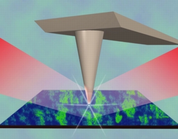 |
| A stylized rendition of an infrared nanoscope illustrates how concentrated infrared illumination finely focuses upon a field just 20-billionths of a meter wide to view metallic puddles in vanadium dioxide as the material begins to transform from an electrically insulating state to an electrically conducting one. |
Abstract:
Images provide clues to Mott transition in semi- and superconductors
Collaboration yields 'the right glasses' for observing mystery behavior in electrons
LOS ALAMOS, NM | Posted on December 13th, 2007In collaboration with the Center for Integrated Nanotechnologies at Los Alamos, an international team of researchers has, for the first time, viewed on a nanoscale the formation of mysterious metallic puddles that facilitate the transition of an electrically insulating material into an electrically conducting one.
The research may lead to a better understanding of superconductors�materials that conduct electricity without energy loss�or development of better materials for powering high-speed electronics.
In a paper published today in Science, Los Alamos researcher Alexander Balatsky joins researchers in describing a novel approach to viewing Mott transition in vanadium dioxide. Balatsky's co-authors include: Mumtaz Qazilbash, Greg Andreev, Brian Maple and Dimitri Basov of the University of California-San Diego; Markus Brehm and Fritz Keilmann of the Max Planck Institute for Biochemistry and Center for NanoScience in Munich, Germany; and Byung-Gyu Chae, Hyun-Tak Kim and Sun Jin Yun of IT Convergence and Components Lab, Electronics and Telecommunication Research Institute in Korea.
Materials such as copper metal contain electrons that are mobile enough to conduct an electrical current. In conducting materials such as copper or aluminum, electrons do not hinder one another and are free to move about the lattice structure of the material. In more-complex crystal oxides, such as vanadium dioxide, electrons can become influenced by nearby positively or negatively charged particles, and their movement can become hindered. These materials are known by physicists as "correlated materials."
Correlated materials include superconductors or semiconductors�crystals peppered or "doped" with atoms that may donate mobile electrons to the solid. Correlated materials can exhibit extraordinary changes in their physical properties, such as transforming from an insulating material to a conducting material, when subjected to relatively small changes in pressure or temperature.
Vanadium dioxide begins to transform itself from an insulator to a conductor when heated above 341 degrees Kelvin (about 154 degrees Fahrenheit or 68 degrees Celsius).
For decades scientists have puzzled over how this transformation to a fully metallic state�known as "Mott" metal-insulator transition�occurs. Balatsky, a Los Alamos condensed-matter theorist, believed, like many other scientists, that the transition begins when metallic puddles begin forming at sites of impurities or imperfections within the lattice. The puddles grow until they touch, and at that point the material becomes conductive, or superconductive.
"We had evidence to believe that metallic puddles were forming in an inhomogenous manner within the material at the transition phase, but we had no way of proving it," said Balatsky. "If you had the right glasses that could see something extremely small, you could see this process occurring."
The �right glasses' came in the form of a microscopic viewing technique known as near-field scanning optical microscopy, which has been used to inspect viruses and nano-transistors. The microscope sees infrared light reflecting off of a surface only 20-billionths of a meter (or 20 nanometers) wide. A single virus is less than 20 nanometers wide, while a typical human hair is about 100,000 nanometers wide.
Using this nanoscale viewer, the UCSD-LANL-Max Planck-ETRI team was able to watch metallic puddles form within vanadium oxide at the exact temperature where the Mott transition was expected to occur. These "infrared nanoscope" images have revealed for the first time a new type of metal "phase" existing only during the transition of the material from its insulating state to its conducting state.
The new findings will help researchers worldwide better describe and understand underlying physical laws of how charges propagate through correlated materials.
The research could help materials scientist understand how to precisely dope a material with specific atoms in order to optimize conducting or superconducting behavior or, conversely, to create materials impervious to electrical conductivity or magnetic influences.
"What is extremely exciting about this research is that four different laboratories with complementary disciplines cooperated to use this infrared nanoscope in its first successful application for solving a solid-state physics puzzle," Keilmann said.
####
About Los Alamos National Laboratory
Los Alamos National Laboratory, a multidisciplinary research institution engaged in strategic science on behalf of national security, is operated by Los Alamos National Security, LLC, a team composed of Bechtel National, the University of California, BWX Technologies, and Washington Group International for the Department of Energy�s National Nuclear Security Administration.
Los Alamos enhances national security by ensuring the safety and reliability of the U.S. nuclear stockpile, developing technologies to reduce threats from weapons of mass destruction, and solving problems related to energy, environment, infrastructure, health, and global security concerns.
Los Alamos National Laboratory/Sandia National Laboratories� Center for Integrated Nanotechnologies is one of five DOE Nanoscale Science Research Centers (NSRCs), premier national user facilities for interdisciplinary research at the nanoscale. Together the NSRCs comprise a suite of complementary facilities that provide researchers with state-of-the-art capabilities to fabricate, process, characterize, and model nanoscale materials, and constitute the largest infrastructure investment of the National Nanotechnology Initiative. The other four NSRCs are located at DOE's Argonne, Brookhaven, Lawrence Berkeley and Oak Ridge National Laboratories. For more information about the DOE NSRCs, please visit http://nano.energy.gov .
For more information, please click here
Contacts:
James E. Rickman
505-665-9203
Copyright © Los Alamos National Laboratory
If you have a comment, please Contact us.Issuers of news releases, not 7th Wave, Inc. or Nanotechnology Now, are solely responsible for the accuracy of the content.
Bookmark:


| Related News Press |
Discoveries
![]() Quantum computer improves AI predictions April 17th, 2026
Quantum computer improves AI predictions April 17th, 2026
![]() Flexible sensor gains sensitivity under pressure April 17th, 2026
Flexible sensor gains sensitivity under pressure April 17th, 2026
![]() A reusable chip for particulate matter sensing April 17th, 2026
A reusable chip for particulate matter sensing April 17th, 2026
![]() Detecting vibrational quantum beating in the predissociation dynamics of SF6 using time-resolved photoelectron spectroscopy April 17th, 2026
Detecting vibrational quantum beating in the predissociation dynamics of SF6 using time-resolved photoelectron spectroscopy April 17th, 2026
Materials/Metamaterials/Magnetoresistance
![]() First real-time observation of two-dimensional melting process: Researchers at Mainz University unveil new insights into magnetic vortex structures August 8th, 2025
First real-time observation of two-dimensional melting process: Researchers at Mainz University unveil new insights into magnetic vortex structures August 8th, 2025
![]() Researchers unveil a groundbreaking clay-based solution to capture carbon dioxide and combat climate change June 6th, 2025
Researchers unveil a groundbreaking clay-based solution to capture carbon dioxide and combat climate change June 6th, 2025
![]() A 1960s idea inspires NBI researchers to study hitherto inaccessible quantum states June 6th, 2025
A 1960s idea inspires NBI researchers to study hitherto inaccessible quantum states June 6th, 2025
![]() Institute for Nanoscience hosts annual proposal planning meeting May 16th, 2025
Institute for Nanoscience hosts annual proposal planning meeting May 16th, 2025
Announcements
![]() A fundamentally new therapeutic approach to cystic fibrosis: Nanobody repairs cellular defect April 17th, 2026
A fundamentally new therapeutic approach to cystic fibrosis: Nanobody repairs cellular defect April 17th, 2026
![]() UC Irvine physicists discover method to reverse �quantum scrambling� : The work addresses the problem of information loss in quantum computing system April 17th, 2026
UC Irvine physicists discover method to reverse �quantum scrambling� : The work addresses the problem of information loss in quantum computing system April 17th, 2026
|
|
||
|
|
||
| The latest news from around the world, FREE | ||
|
|
||
|
|
||
| Premium Products | ||
|
|
||
|
Only the news you want to read!
Learn More |
||
|
|
||
|
Full-service, expert consulting
Learn More |
||
|
|
||