Home > Press > NIST Imaging System Maps Nanomechanical Properties
 |
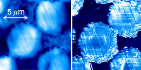
| An atomic force microscope normally reveals the topography of a composite material (l.) NIST's new apparatus adds software and electronics to map nanomechanical properties (r.) The NIST system reveals that the glass fibers are stiffer than the surrounding polymer matrix but sometimes soften at their cores.
Credit: DC Hurley/NIST |
Abstract:
The National Institute of Standards and Technology (NIST) has developed an imaging system that quickly maps the mechanical properties of materials—how stiff or stretchy they are, for example—at scales on the order of billionths of a meter. The new tool can be a cost-effective way to design and characterize mixed nanoscale materials such as composites or thin-film structures.
NIST Imaging System Maps Nanomechanical Properties
GAITHERSBURG, MD | Posted on December 12th, 2007The NIST nanomechanical mapper uses custom software and electronics to process data acquired by a conventional atomic force microscope (AFM), transforming the microscope's normal topographical maps of surfaces into precise two-dimensional representations of mechanical properties near the surface. The images enable scientists to see variations in elasticity, adhesion or friction, which may vary in different materials even after they are mixed together. The NIST system, described fully for the first time in a new paper,* can make an image in minutes whereas competing systems might take an entire day.
The images are based on measurements and interpretations of changes in frequency as a vibrating AFM tip scans a surface. Such measurements have commonly been made at stationary positions, but until now 2D imaging at many points across a sample has been too slow to be practical. The NIST DSP-RTS system (for digital signal processor-based resonance tracking system) has the special feature of locking onto and tracking changes in frequency as the tip moves over a surface. Mechanical properties of a sample are deduced from calculations based on measurements of the vibrational frequencies of the AFM tip in the air and changes in frequency when the tip contacts the material surface.
NIST materials researchers have used the system to map elastic properties of thin films with finer spatial resolution than is possible with other tools. The DSP-RTS can produce a 256 × 256 pixel image with micrometer-scale dimensions in 20 to 25 minutes. The new system also is modular and offers greater flexibility than competing approaches. Adding capability to map additional materials properties can be as simple as updating the software.
* A.B. Kos and D.C. Hurley. Nanomechanical mapping with resonance tracking scanned probe microscope. Measurement Science and Technology 19 (2008) 015504.
####
About NIST
From automated teller machines and atomic clocks to mammograms and semiconductors, innumerable products and services rely in some way on technology, measurement, and standards provided by the National Institute of Standards and Technology.
Founded in 1901, NIST is a non-regulatory federal agency within the U.S. Department of Commerce. NIST's mission is to promote U.S. innovation and industrial competitiveness by advancing measurement science, standards, and technology in ways that enhance economic security and improve our quality of life.
For more information, please click here
Contacts:
Laura Ost
(303) 497-4880
Copyright © NIST
If you have a comment, please Contact us.Issuers of news releases, not 7th Wave, Inc. or Nanotechnology Now, are solely responsible for the accuracy of the content.
| Related News Press |
Materials/Metamaterials/Magnetoresistance
![]() First real-time observation of two-dimensional melting process: Researchers at Mainz University unveil new insights into magnetic vortex structures August 8th, 2025
First real-time observation of two-dimensional melting process: Researchers at Mainz University unveil new insights into magnetic vortex structures August 8th, 2025
![]() Researchers unveil a groundbreaking clay-based solution to capture carbon dioxide and combat climate change June 6th, 2025
Researchers unveil a groundbreaking clay-based solution to capture carbon dioxide and combat climate change June 6th, 2025
![]() A 1960s idea inspires NBI researchers to study hitherto inaccessible quantum states June 6th, 2025
A 1960s idea inspires NBI researchers to study hitherto inaccessible quantum states June 6th, 2025
![]() Institute for Nanoscience hosts annual proposal planning meeting May 16th, 2025
Institute for Nanoscience hosts annual proposal planning meeting May 16th, 2025
Announcements
![]() A fundamentally new therapeutic approach to cystic fibrosis: Nanobody repairs cellular defect April 17th, 2026
A fundamentally new therapeutic approach to cystic fibrosis: Nanobody repairs cellular defect April 17th, 2026
![]() UC Irvine physicists discover method to reverse ‘quantum scrambling’ : The work addresses the problem of information loss in quantum computing system April 17th, 2026
UC Irvine physicists discover method to reverse ‘quantum scrambling’ : The work addresses the problem of information loss in quantum computing system April 17th, 2026
Tools
![]() Metasurfaces smooth light to boost magnetic sensing precision January 30th, 2026
Metasurfaces smooth light to boost magnetic sensing precision January 30th, 2026
![]() From sensors to smart systems: the rise of AI-driven photonic noses January 30th, 2026
From sensors to smart systems: the rise of AI-driven photonic noses January 30th, 2026
![]() Japan launches fully domestically produced quantum computer: Expo visitors to experience quantum computing firsthand August 8th, 2025
Japan launches fully domestically produced quantum computer: Expo visitors to experience quantum computing firsthand August 8th, 2025
|
|
||
|
|
||
| The latest news from around the world, FREE | ||
|
|
||
|
|
||
| Premium Products | ||
|
|
||
|
Only the news you want to read!
Learn More |
||
|
|
||
|
Full-service, expert consulting
Learn More |
||
|
|
||


