Home > Press > Veeco Wins Key Competitive Evaluation
Abstract:
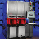
Veeco Instruments Inc. announced today a significant competitive Metrology win for its Dimension X Atomic Force Microscope from a leading international semiconductor DRAM manufacturer.
Veeco Atomic Force Microscope Wins Key Competitive Evaluation at Semiconductor Customer
Woodbury, NY. October 15, 2004
Veeco Instruments Inc. announced today a significant competitive Metrology win for its Dimension X Atomic Force Microscope from a leading international semiconductor DRAM manufacturer. After a detailed side-by-side evaluation against a new, competitive AFM offering, the Veeco Dimension X was selected for the manufacturer's critical DRAM etch metrology applications for both current and future technology nodes.
Don Kania, Ph.D., President of Veeco, commented, "With 200 tools in semi wafer fabs, we incorporated years of AFM experience into our second-generation platform, the Dimension X. Our continued success is the result of Veeco's depth of expertise and superior AFM technology."

|

|
Paul Clayton, Vice President, General Manager of Veeco's Automated AFM Group added, "During the side-by-side evaluation, Veeco's Dimension X proved to have superior cost of ownership, higher throughput, and extendibility to 70nm. We demonstrated better reproducibility that will enable the customer to utilize our AFMs for the next technology node in both their 200mm and 300mm fabs. Immediately following the evaluation, Veeco's AFM is being put into production."
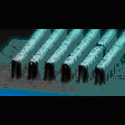
The Dimension X is designed specifically to address the semiconductor industry's need for higher-resolution etch depth metrology. It enables chipmakers to measure etch related structures that are 90nm and below for depth uniformity control in high volume production environments. The gauge-capable system gives users the ability to take repeatable, in-line measurements of shallow trench isolation (STI), as well as contacts and vias in high aspect ratio depth metrology without damaging the device or sacrificing a wafer for cross-sectioned measurements. The Dimension's proven 200 mm and 300mm automation platforms have been adopted by fabs worldwide for their reliability, improved throughput, unparalleled repeatability and low cost of ownership.
About Veeco
Veeco Instruments Inc. provides solutions for nanoscale applications in the worldwide, data storage, compound semiconductor/wireless, semiconductor and scientific research markets. Our Metrology products are used to measure at the nanoscale and our Process Equipment tools help create nanoscale devices. Veeco's manufacturing and engineering facilities are located in New York, New Jersey, California, Colorado, Arizona and Minnesota. Global sales and service offices are located throughout the United States, Europe, Japan and Asia Pacific. Additional information on Veeco can be found at www.veeco.com.
To the extent that this news release discusses expectations about market condition, market acceptance and future sales of Veeco's products, Veeco's future financial performance, or otherwise makes statements about the future, such statements are forward-looking and are subject to a number of risks and uncertainties that could cause actual results to differ materially from the statements made. These factors include the cyclical nature of the compound semiconductor/wireless, data storage, semiconductor and research markets, risks associated with integrating acquired businesses and the acceptance of new products by individual customers and by the marketplace and other factors discussed in the Business Description and Management's Discussion and Analysis sections of Veeco's Annual Report on Form 10-K, subsequent Quarterly Reports on Form 10-Q and current reports on Form 8-K.
Debra Wasser
516-677-0200, ext.1472
Trade Contact:
Joan Horwitz
Director of Marketing Communications
805-967-2700, x2476
Copyright © Veeco Instruments
If you have a comment, please us.
Issuers of news releases, not 7th Wave, Inc. or Nanotechnology Now, are solely responsible for the accuracy of the content.
| Related News Press |
Announcements
![]() A fundamentally new therapeutic approach to cystic fibrosis: Nanobody repairs cellular defect April 17th, 2026
A fundamentally new therapeutic approach to cystic fibrosis: Nanobody repairs cellular defect April 17th, 2026
![]() UC Irvine physicists discover method to reverse �quantum scrambling� : The work addresses the problem of information loss in quantum computing system April 17th, 2026
UC Irvine physicists discover method to reverse �quantum scrambling� : The work addresses the problem of information loss in quantum computing system April 17th, 2026
Tools
![]() Metasurfaces smooth light to boost magnetic sensing precision January 30th, 2026
Metasurfaces smooth light to boost magnetic sensing precision January 30th, 2026
![]() From sensors to smart systems: the rise of AI-driven photonic noses January 30th, 2026
From sensors to smart systems: the rise of AI-driven photonic noses January 30th, 2026
![]() Japan launches fully domestically produced quantum computer: Expo visitors to experience quantum computing firsthand August 8th, 2025
Japan launches fully domestically produced quantum computer: Expo visitors to experience quantum computing firsthand August 8th, 2025
|
|
||
|
|
||
| The latest news from around the world, FREE | ||
|
|
||
|
|
||
| Premium Products | ||
|
|
||
|
Only the news you want to read!
Learn More |
||
|
|
||
|
Full-service, expert consulting
Learn More |
||
|
|
||


