Home > Nanotechnology Columns > UAlbany College of Nanoscale Science and Engineering > CNSE's Novel Semiconductor Research and Development Options for Rapid Commercialization
 |
Michael Liehr CNSE Associate Vice President for Business, Alliances and Consortia; Professor at CNSE University at Albany - College of Nanoscale Science & Engineering |
Abstract:
The development of commercial CMOS base technologies and derivative features is aimed at high volume production objectives which justify the very significant development and capital expenditures required. Novel materials and device concepts developed at universities, on the other hand, typically lack access to state-of-the-art 300mm wafer processing capability required for rapid insertion of such concepts into the mainstream manufacturing menu. The College of Nanoscale Science and Engineering (CNSE) in Albany provides an environment that bridges the gap between university research opportunities and manufacturing implementation. Two new options for commercial engagements at CNSE are described in this paper.
August 25th, 2010
CNSE's Novel Semiconductor Research and Development Options for Rapid Commercialization
The development of commercial CMOS base technologies and derivative features is aimed at high volume production objectives which justify the very significant development and capital expenditures required. Novel materials and device concepts developed at universities, on the other hand, typically lack access to state-of-the-art 300mm wafer processing capability required for rapid insertion of such concepts into the mainstream manufacturing menu. The College of Nanoscale Science and Engineering (CNSE) in Albany provides an environment that bridges the gap between university research opportunities and manufacturing implementation. Two new options for commercial engagements at CNSE are described in this paper.
Integrated CMOS Capability
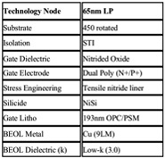
While leading-edge process elements are being developed at the 22nm technology node and beyond, CNSE is also offering customized research and development of process features and derivatives integrated into a fully design enabled CMOS process flow. Toward this end, CNSE is using a low-power, industry standard bulk 65nm technology [Table 1].
 |
| Table 1. Bulk CMOS capability at CNSE (courtesy of IBM). |
65nm industry standard bulk CMOS is the node which currently attracts most design attention in the commercial space. The technology features dual poly gates with multiple threshold voltage options and a thick oxide compatible with 1.8V to 3.3V circuit operation. Back-end-of-the-line metallurgy is Cu-based and allows the use of low-K materials for insulators. The technology is enhanced with and radio-frequency (RF) passive elements, such as resistors, capacitors and inductors using existing back end metallurgy with minimal to no manufacturing cost adders.
Unique opportunities exist at CNSE to develop process features that require the introduction of novel materials, a typically difficult challenge in a more traditional manufacturing environment. While CNSE follows industry standard procedures for contamination control, the research and development nature of the facility lends itself to explore integration of unique process elements involving materials not proven to be compatible with standard CMOS, such as resistive random access memory (Re-RAM) or spin-based memory elements. As an example and as part of an on-going, more future-oriented research project, CNSE is introducing graphene into the cleanroom, which involves addressing contamination control issues due to the nature of the catalytic growth conditions used to grow graphene.
In 2010, the College is expanding its facilities and partners to build a Packaging Center on campus that will initially focus on the development on 300mm wafer-scale 3-dimensional (3D) integration. In collaboration with partners, this capability allows heterogeneous integration of electro-mechanical system (MEMS), sensors, optical components and RF applications.
The use of 65nm bulk CMOS in this "More Moore" application enables prototype 3D application development on industry standard CMOS technologies with subsequent seamless transfer of the product into Foundry-based volume manufacturing. The program is enhanced with a Multi-Project-Wafer program, which allows access to the technology while maintaining a financially attractive infrastructure access.
Dr. Liehr's Bio
|
|
||
|
|
||
| The latest news from around the world, FREE | ||
|
|
||
|
|
||
| Premium Products | ||
|
|
||
|
Only the news you want to read!
Learn More |
||
|
|
||
|
Full-service, expert consulting
Learn More |
||
|
|
||


