Home > Nanotechnology Columns > NT-MDT > Piezoresponse Force Microscopy: Imaging Materials from Biology through to Electronics
 |
Vladimir Savin NT-MDT |
Abstract:
The electro-mechanical coupling behaviour of many materials in systems from bio
based cell membranes and proteins to ferroelectric and piezoelectric electronic materials can now be analysed in great detail via Piezoresponse Force Microscopy (PFM).
February 25th, 2010
Piezoresponse Force Microscopy: Imaging Materials from Biology through to Electronics
The electro-mechanical coupling behaviour of many materials in systems from bio
based cell membranes and proteins to ferroelectric and piezoelectric electronic materials can now be analysed in great detail via Piezoresponse Force Microscopy (PFM). This imaging technique is of particular interest in the development of novel electronic devices for example those based on ferroelectric domain switching – systems of great potential for future developments in areas such as computer memory. PFM uses a scanning force microscope operating in the contact mode with an alternating voltage applied to the probe tip (see Fig 1). This technique is particularly attractive as it has a high lateral resolution of only ~10-20 nm together with an astonishing sensitivity of ~0.1 pm/V.
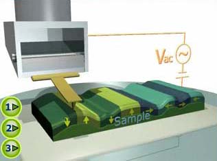 |
Fig 1. Schematic set-up of a scanning force probe operating as a Piezoresponse Force Microscope. If you’d like to see full animations, please, visit this page. For in-depth information on how NTEGRA nanolaboratory can be used for investigation of low-voltage memories in PFM see Nature Materials 8, 62 - 67 (2009)
The imaging of ferroelectric domains using this technique is possible due to the fact that ferroelectric behaviour implies piezoelectricity, and consequently mapping the piezoelectric response of a material provides a direct image of its ferroelectric domain structure.
Hexagonal Domains in Lithium Niobate
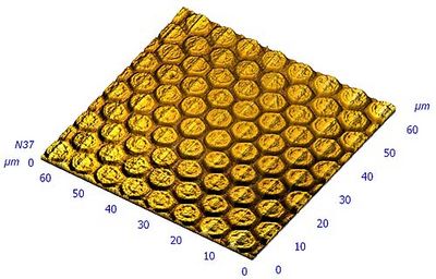 |
Fig 2.The image illustrates the hexagonal domain structure of Lithium Niobate – a structure typically produced by the room temperature electric field poling. Lithium Niobate is an important material for use in telecommunications and optical devices such as wave guides and modulators.The sample was kindly given by C. Gawith, Optoelectronics Research Centre University of Southampton. Image courtesy of T. Jungk, A. Hoffmann, E. Soergel, University of Bonn.
Ferroelectric Domain Patterns in Multiferroic Manganite
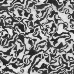 |
Fig 3.The image was produced from the polished surface of a z-cut ferroelectric single crystal using PFM. The irregular nature of the image illustrates breaking ferroelectric order by the random fields. Scan size 50 x 50 μm, produced using a NTEGRA Solaris system with AFM head. The sample was kindly given by Dr. M. Fiebig. Image Courtesy Dr. T. Jungk, Dr. F. Johann, Dr. A. Hoffmann, Dr. E. Soergel, University of Bonn, Germany
The Equipment
A typical PFM set-up would utilise NTEGRA Aura image recording with DCP11 probes.
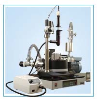 |
Fig 4. Probe NanoLaboratory NTEGRA Aura is intended for studies in the conditions of controlled environment and low vacuum.
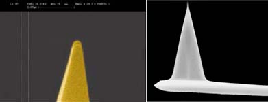 |
Fig 5. DCP 11 Probe. Left picture – tip with diamond coating. Typical curvature radius of a tip: 70 nm. Right picture: tip height: 10 - 15 μm.
|
|
||
|
|
||
| The latest news from around the world, FREE | ||
|
|
||
|
|
||
| Premium Products | ||
|
|
||
|
Only the news you want to read!
Learn More |
||
|
|
||
|
Full-service, expert consulting
Learn More |
||
|
|
||


