Home > Nanotechnology Columns > Kos Galatsis > The Gangsters of Nanoelectronics: Power and Variability
 |
Kos Galatsis Chief Operating Officer FENA and WIN Centers, UCLA |
Abstract:
The semiconductor industry is extremely sophisticated. It is one of the few industries that meticulously maps out their future, identifying and predicting challenges ahead. Most of this foresight is captured in the numerous chapters of the International Roadmap for Semiconductors (ITRS) which is a collective effort of semiconductor experts from around the world. There are numerous challenges that touch upon shortfalls in materials, devices, lithography, interconnects, integration and assembly, among others. Most of these challenges deal with fundamental nanotechnology limits as determined by the laws of thermodynamics and quantum mechanics. The greatest challenge that faces nanoelectronics is the prolific demise of transistor scaling, otherwise known as Moore's Law. The cause of this real fear comes from what I call the gangsters of nanoelectroincs. These are a) power dissipation, which elevates on-chip temperatures degrading chip performance and b) device-level variabilities, that make circuits unreliable and create design difficulties for engineers. There are many technologies cooking to circumvet these challenges, I present a few within this article.
October 5th, 2007
The Gangsters of Nanoelectronics: Power and Variability
With such gangsters plaguing the semiconductor industry's future, two potential paths forward are clear. One path is to continue increasing chip-scale functional throughput by looking at new functional materials at atomic and molecular levels for assembly into new low power devices - possibly with different logic state variables that can better tolerate variabilities. The second distinct approach is to increase chip-scale functionality by exploiting the heterogeneous integration of materials, such as compound semiconductors on silicon, or various other materials such as nanowires, tubes and graphene. Based on these two paths forward, some developments worth keeping under your radar are:
1) Molecular Electronics - As reported in Nature (2006) from both Heath and Stoddart groups, using the cross-bar architecture and engineering molecules to self assembly at crosspoint junctions could be a feasible path forward to chip memory densities greater than 10E11 (currently we are at 10E9). Such memory elements would reduce power consumption and due to the sheer density, would provide the ability for numerous fault tolerant schemes to be implemented.
 |
| Cross bar architecture with bi-state molecules self-assembled at crosspoints. Lines are 16nm wide. |
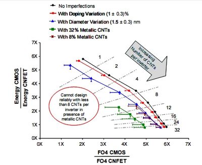
2) Carbon Nanotubes (CNT) - CNTs have made some solid progress in device and circuit maturity. For instance, HSP Wong (Stanford) presented at the International Solid State Circuits Conference 2007 sophisticated developments of CNT based circuit design. He showed the trade-offs required to ensure a feasible CNT device operation with respect to energy and delay time as compared to CMOS. This study shows how ballistic electron transport could be superior to existing diffusion based transport. By optimizing device specs such as the number of CNT's, doping variation, diameter variation and ratio between metallic and semiconducting tubes, it is possible for a CNT based FET inverter manufactured using a perfect CNFET technology to have 5.1 times faster delay and 2.6 times lower energy per cycle compared to a 32nm silicon CMOS inverter.
 |
| Relationship of delay and energy tradeoffs normalized to CMOS of a CNT based inverter. |
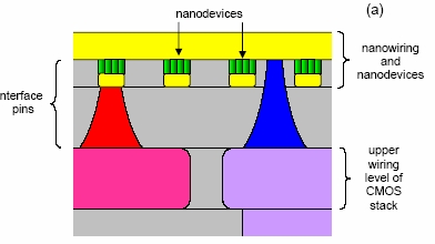
3) Alternative Architecture - Other than optimizing materials and devices, architectures have a lot to do with how power and variability affect overall chip throughput, yield and performance. A novel idea by Likharev (SUNY) shows how an architecture can take the best of both worlds, that being CMOS logic (logic) and MOLecular memory to create a hybrid architecture called CMOL. This architecture combines both logic and memory which reduces traditional Von Neumann bus bottlenecks and reducing power dissipation in interconnects. Simulations have shown that CMOL can out perform CMOS in applications such as image recognition by many times and be extremely fault tolerant.
 |
| A schematic of the CMOL architecture. |
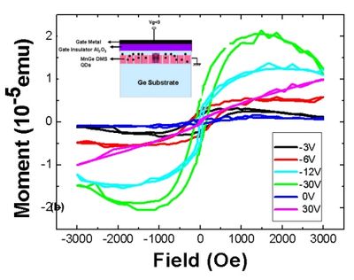
4) New State Variables - New state variable technologies such as spintronics is gaining momentum, and for good reasons. Spintronics has the ability to reduce overall power consumption by eliminating the need for electron movement. Doing so reduces scattering and hence unnecessary power dissipation. Demonstration of room temp phase transition between ferromagnetic and paramagnetism has been key in foreseeing a future for silicon electronics to possibly becoming "spin" enabled. K.L. Wang (UCLA) was first to demonstrate in 2006 (APL) a ferromagnetic phase transition in Group IV materials. What this means is that there is solid hope of spintronics being integrated into other Group IV materials such as silicon which would be less sensitive to variabilities as a result of the inherent collective behavior between spin carriers.
 |
| The transition of MnGe from Ferro to Parra via electric field influence. |
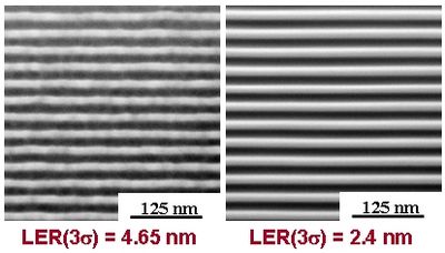
5) Patterning - Di-block copolymers can be used as photoresist replacing the existing PMMA resists used in chip manufacturing. Impressive results from Nealey's group in 2006 published in Materials Today shows Line Edge Roughness improvement by 2x. This means structures can be made with specs closer to ideal, which would then make device performance more predictable and overall chip yields higher.
 |
| A comparison between PMMA (left) and di-block copolymer technology |
The gangsters of nanoelectronics will face some serious competition fighting up against increased R&D budgets together with the tough gloves of innovative engineers and scientists. In the meantime, I wait to see how well we do in ramping the 32nm node technology and further challenges our teams face in 22nm node development.
|
|
||
|
|
||
| The latest news from around the world, FREE | ||
|
|
||
|
|
||
| Premium Products | ||
|
|
||
|
Only the news you want to read!
Learn More |
||
|
|
||
|
Full-service, expert consulting
Learn More |
||
|
|
||


